Engineers discover natural 'workbench' for nanoscale construction
The findings appear in the August issue of Nature Materials.
Alerted by an unusual diffraction effect of a common ceramic material, researchers used imaging to identify a two-phase structural pattern ideal as the first step towards nanodevice construction. Practical application of nanotechnology will rely upon engineering’s ability to manipulate atoms and molecules into long-range order to produce materials with desired functionalities. The Penn findings provide a simpler method for the ordering of composite parts on the nanometer scale, which is integral to the incorporation of nano-objects such as particles and wires that make up nanodevices.
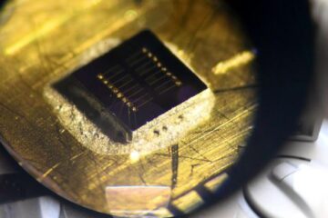
The material used in the Penn study is an ionically- conductive, crystalline ceramic (Nd2/3-xLi3x)TiO3 that engineers observed with transmission electron microscopy. The powdered perovskite exhibited two distinct patterns at the atomic scale with identical periodicity: a nanoscale chessboard pattern and a diamond pattern that indicated periodic separation into two phases within the structure. This spontaneous separation of phases could present a new foundation on which to build nanodevice technology. This material – made using standard and easily reproducible ceramic processing methods – represents the formation of a spontaneous microscopic surface controlled on the nanoscale with atomic precision.
Further study revealed that the separation of the structure into two distinct phases was a result of the oxide separating into lithium rich squares and lithium poor stripes. By varying the amount of lithium and neodymium, two ingredients in the ceramic powder, engineers controlled the length and spacing of the alternating phases, thereby tuning the workbench upon which nanodevices could be built.
On a larger-than-atomic scale, the research extends science’s knowledge of the properties of a most common oxide structure type, currently used for superconducting materials, magnetoresistive materials and ferroelectrics.
“This study represents great potential for the use of standard ceramic processing methods for nanotechnology,” said Peter K. Davies, chair of the Department of Materials Science and Engineering at Penn. “The phase separation occurs spontaneously, providing two phases whose dimensions both extend into the nanometer scale. This unique feature could lead to its application as a template for the assembly of nanostructures or molecular monolayers.”
Media Contact
More Information:
http://www.upenn.eduAll latest news from the category: Materials Sciences
Materials management deals with the research, development, manufacturing and processing of raw and industrial materials. Key aspects here are biological and medical issues, which play an increasingly important role in this field.
innovations-report offers in-depth articles related to the development and application of materials and the structure and properties of new materials.


Newest articles

Sea slugs inspire highly stretchable biomedical sensor
USC Viterbi School of Engineering researcher Hangbo Zhao presents findings on highly stretchable and customizable microneedles for application in fields including neuroscience, tissue engineering, and wearable bioelectronics. The revolution in…

Twisting and binding matter waves with photons in a cavity
Precisely measuring the energy states of individual atoms has been a historical challenge for physicists due to atomic recoil. When an atom interacts with a photon, the atom “recoils” in…
Nanotubes, nanoparticles, and antibodies detect tiny amounts of fentanyl
New sensor is six orders of magnitude more sensitive than the next best thing. A research team at Pitt led by Alexander Star, a chemistry professor in the Kenneth P. Dietrich…

