Optimisation of 3D printing of optically active nanostructures
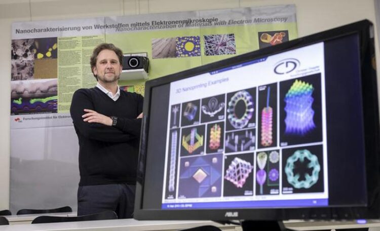
Harald Plank from the Institute of Electron Microscopy and Nanoanalysis at TU Graz has been researching for over ten years how complex, free-standing 3D architectures can be produced in the nanometre range.
Credit: Lunghammer - TU Graz
The shape, size and optical properties of 3-dimensional nanostructures can now be simulated in advance before they are produced directly with high precision on a wide variety of surfaces.
For around 20 years, it has been possible to modify surfaces via nanoparticles so that they concentrate or manipulate light in the desired way or trigger other reactions. Such optically active nanostructures can be found in solar cells and biological or chemical sensors, for example. In order to expand their range of applications, researchers at the Institute of Electron Microscopy and Nanoanalysis (Graz University of Technology) and the Graz Centre of Electron Microscopy (ZFE) have been working for more than one decade on manufacturing not only flat nanostructures, but in particular complex, free-standing 3D architectures. The team led by Harald Plank, Verena Reisecker and David Kuhness has achieved two breakthroughs. It is now possible to precisely simulate the required shapes and sizes of nanostructures in advance to achieve the desired optical properties, which can then be accurately produced. They have also managed to completely remove chemical impurities, incorporated during initial production without negatively impacting the 3D nanoarchitectures.
Trial-and-error procedure becomes unnecessary
Until now, three-dimensional nanostructures required a time consuming trial-and-error process until the product revealed the desired optical properties. This effort has finally been eliminated. “The consistency between simulations and real plasmonic resonances of a wide range of nanoarchitectures is very high,” explains Harald Plank. “This is a huge step forward. The hard work of the last few years has finally paid off.” The technology is currently the only one in the world that can be used to produce complex 3-dimensional structures with individual features smaller than 10 nanometres in a controlled, single step procedure on almost any surface. For comparison, the smallest viruses are around 20 nanometres in size. “The biggest challenge in recent years was to transfer the 3D architectures into high-purity materials without destroying the morphology,” explains Harald Plank. “This development leap enables new optical effects and application concepts thanks to the 3D aspect.” Nanoprobes or optical tweezers with sizes in the nanometre range are now within reach.
Precisely controlled electron beam
The researchers use focused electron beam induced deposition to produce the nanostructures. The relevant surface is exposed to special gases under vacuum conditions. A finely focused electron beam splits the gas molecules, whereupon parts of them change into a solid state and adhere to the desired location. “By precisely controlling beam movements and exposure times, we are able to produce complex nanostructures with lattice- or sheet-like building blocks in a single step”, explains Harald Plank. By stacking these nano-volumes on top of each other, three-dimensional structures can ultimately be constructed.
This research area is anchored in the Field of Expertise “Advanced Materials Science“, one of five strategic foci of TU Graz.
Journal: Advanced Functional Materials
DOI: 10.1002/adfm.202310110
Method of Research: Experimental study
Subject of Research: Not applicable
Article Title Spectral Tuning of Plasmonic Activity in 3D Nanostructures via High-Precision Nano-Printing
Article Publication Date: 1-Nov-2023
Media Contact
Philipp Jarke
Graz University of Technology
philipp.jarke@tugraz.at
Office: +43 316 873 4566
Original Source
Media Contact
All latest news from the category: Materials Sciences
Materials management deals with the research, development, manufacturing and processing of raw and industrial materials. Key aspects here are biological and medical issues, which play an increasingly important role in this field.
innovations-report offers in-depth articles related to the development and application of materials and the structure and properties of new materials.


Newest articles

Sea slugs inspire highly stretchable biomedical sensor
USC Viterbi School of Engineering researcher Hangbo Zhao presents findings on highly stretchable and customizable microneedles for application in fields including neuroscience, tissue engineering, and wearable bioelectronics. The revolution in…

Twisting and binding matter waves with photons in a cavity
Precisely measuring the energy states of individual atoms has been a historical challenge for physicists due to atomic recoil. When an atom interacts with a photon, the atom “recoils” in…
Nanotubes, nanoparticles, and antibodies detect tiny amounts of fentanyl
New sensor is six orders of magnitude more sensitive than the next best thing. A research team at Pitt led by Alexander Star, a chemistry professor in the Kenneth P. Dietrich…

