Dual microscopes illuminate electronic switching speeds
Designers of semiconductor devices are like downhill skiers – they thrive on speed. And achieving speed in the semiconductor business is all about the stuff you start with. While silicon is still the mainstay of the industry, circuit designers also would like to put materials like gallium nitride and silicon carbide into wider use. Such advanced semiconductor materials can operate at higher voltages and provide faster switching speeds, an important characteristic in determining how fast a semiconductor circuit can process information.
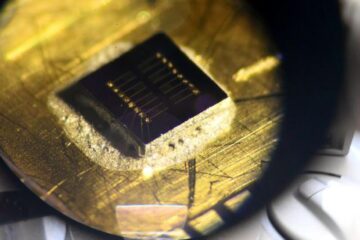
Reporting in the Sept. 22 issue of Applied Physics Letters, a National Institute of Standards and Technology (NIST) researcher and a Korean guest researcher describe a new method for scanning semiconductors for defects that may help accelerate the market for these newer materials. The duo combined an atomic force microscope with a scanning capacitance microscope and then added custom software and a simple on/off switch for the AFM’s positioning laser.
The result is an instrument that can measure how fast a material generates electrical charges and then map those speeds in sections (at least for gallium nitride) that are only about 100 nanometers square. Current methods for measuring switching speed (carrier lifetime) produce only bulk averages.
According to NIST co-developer Joseph Kopanski, the system allows quick scanning of semiconductor wafers for defects that otherwise may not be found until an expensive device has already been built on the material. Most defects in semiconductors (i.e. sections with missing atoms) are presumed to slow down the speed that charges move through a material. Kopanski says further research using the new technique should determine if this assumption is correct. A patent application is pending on the technique.
Media Contact
More Information:
http://www.nist.gov/All latest news from the category: Information Technology
Here you can find a summary of innovations in the fields of information and data processing and up-to-date developments on IT equipment and hardware.
This area covers topics such as IT services, IT architectures, IT management and telecommunications.


Newest articles

Sea slugs inspire highly stretchable biomedical sensor
USC Viterbi School of Engineering researcher Hangbo Zhao presents findings on highly stretchable and customizable microneedles for application in fields including neuroscience, tissue engineering, and wearable bioelectronics. The revolution in…

Twisting and binding matter waves with photons in a cavity
Precisely measuring the energy states of individual atoms has been a historical challenge for physicists due to atomic recoil. When an atom interacts with a photon, the atom “recoils” in…
Nanotubes, nanoparticles, and antibodies detect tiny amounts of fentanyl
New sensor is six orders of magnitude more sensitive than the next best thing. A research team at Pitt led by Alexander Star, a chemistry professor in the Kenneth P. Dietrich…

