Exciton dynamics for future ultra-high-speed communication
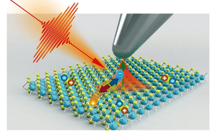
Time-resolved STM (TR-STM) setup for measuring carrier dynamics in TMDCs.
Credit: University of Tsukuba
… studied at unprecedented resolution:
Researchers from the University of Tsukuba and collaborating partners have observed fine-scale exciton dynamics in atomically thin layered materials. This basic study for future optical communications could help replace charge transfer as the standard communications tool.
Future optical communication that’s vastly more reliable and faster than what’s commonly available today will require new technology. Modern communication is based on charge transfer, which can result in large transmission losses during certain data-intensive applications. Excitons are alternatives, yet they face technical challenges for widespread implementation. Now, researchers from Japan have overcome a critical bottleneck that might give rise to ultrafast optical communication technology based on excitons.
Researchers are excited about using excitons—assemblies of bound electrons and holes—for terabits per second optical communication. Unfortunately, rapid exciton dissociation at room temperature in conventional three-dimensional semiconductors precludes immediate practical applications. However, atomically thin layered two-dimensional materials (transition metal dichalcogenides, TMDCs) impart certain advantages. For example, in TMDCs, excitons can be stable at room temperature and can travel long distances. Local, ultrasmall-scale defects are inevitable in TMDCs—yet might even be advantageous if researchers can understand the role of such defects on the dynamics of exciton transport, and thus the properties of TMDC-based devices.
Understanding the nanoscale dynamics of excitons in TMDCs will help answer such questions. “Commonly used technologies have insufficient resolution,” explains Professor Hiroyuki Mogi, lead author, “but our scanning tunneling microscopy approach changes this. To optimize imaging resolution, we applied a bias voltage in a manner that dissociates the underlying excitons, at a resolution of several nanometers.”
The researchers’ focus was on how nanostructures—such as grain boundaries and ripples&mdashin TMDCs modulated exciton dynamics. A highlight of the research is that grain boundaries corresponded to enhanced exciton recombination within ~8 nanometers. Another highlight is that ripples corresponded to decreased exciton binding energy, and smaller ripples corresponded to a longer exciton lifetime than larger ripples. These results confirm theoretical predictions that prior researchers had been unable to experimentally verify.
“The 2.5-nanometer spatial resolution of our technique is groundbreaking,” says Professor Hidemi Shigekawa, senior author. “At this resolution, we confirmed that in the tungsten diselenide region, the rate of exciton-exciton annihilation was 0.10 ± 0.02 square centimeters per second, and was modulated by local nanostructures.”
Based on the research described here, excitons will become an essential tool to remove many current barriers to remote communication. In the future, that is expected to expand real-life applications of advanced optical communications—such as seamless business and financial data-sharing that speeds up operations, faster search-and-rescue operations based on artificial intelligence image-processing of airborne drone data, and safer driverless vehicles.
We acknowledge the financial support of a Grant-in-Aid for Scientific Research from Japan Society for the Promotion of Science (17H06088, 20H00341) and Japan Core Research Evolutional Science and Technology (CREST) (JPMJCR1875, JPMJCR16F3).
Original Paper
The article, “Ultrafast nanoscale exciton dynamics via laser-combined scanning tunnelling microscopy in atomically thin materials,” was published in npj 2D Materials and Applications at DOI: 10.1038/s41699-022-00345-1
Correspondence
Professor SHIGEKAWA Hidemi
Assistant Professor MOGI Hiroyuki
R&D Center for Innovative Material Characterization/ Department of Applied Physics, Faculty of Pure and Applied Sciences, University of Tsukuba
Related Link
Faculty of Pure and Applied Sciences
R&D Center for Innovative Material Characterization
Journal: npj 2D Materials and Applications
DOI: 10.1038/s41699-022-00345-1
Article Title: Ultrafast nanoscale exciton dynamics via laser-combined scanning tunneling microscopy in atomically thin materials
Article Publication Date: 14-Oct-2022
Media Contact
KAMOSHITA Kimio
University of Tsukuba
kohositu@un.tsukuba.ac.jp
Original Source
All latest news from the category: Information Technology
Here you can find a summary of innovations in the fields of information and data processing and up-to-date developments on IT equipment and hardware.
This area covers topics such as IT services, IT architectures, IT management and telecommunications.


Newest articles
Recovering phosphorus from sewage sludge ash
Chemical and heat treatment of sewage sludge can recover phosphorus in a process that could help address the problem of diminishing supplies of phosphorus ores. Valuable supplies of phosphorus could…
Efficient, sustainable and cost-effective hybrid energy storage system for modern power grids
EU project HyFlow: Over three years of research, the consortium of the EU project HyFlow has successfully developed a highly efficient, sustainable, and cost-effective hybrid energy storage system (HESS) that…
After 25 years, researchers uncover genetic cause of rare neurological disease
Some families call it a trial of faith. Others just call it a curse. The progressive neurological disease known as spinocerebellar ataxia 4 (SCA4) is a rare condition, but its…

