Penn Study: Understanding Graphene’s Electrical Properties on an Atomic Level
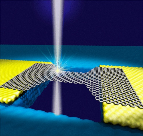
An illustration of a graphene nanoribbon shaped by the beam of a transmission electron microscope. (Credit: Robert Johnson)
Now, for the first time, researchers from the University of Pennsylvania have used a cutting-edge microscope to study the relationship between the atomic geometry of a ribbon of graphene and its electrical properties.
A deeper understanding of this relationship will be necessary for the design of graphene-based integrated circuits, computer chips and other electronic devices.
The study was led by professors A.T. Charlie Johnson and Marija Drndić, both of the Department of Physics and Astronomy in Penn’s School of Arts & Sciences, along with Zhengqing John Qi, a member of Johnson’s lab, and Julio Rodríguez-Manzo from Drndic’s lab. Sung Ju Hong, then a member of Johnson’s lab, also contributed to the study.
The Penn team collaborated with researchers at Brookhaven National Laboratory, the Université Catholique de Louvain in Belgium and Seoul National University in South Korea.
Their study was published in the journal Nano Letters.
The team’s experiments were enabled by Brookhaven’s aberration-corrected transmission electron microscope, or AC-TEM. By focusing the microscope’s electron beam, the researchers were able to controllably cut sheets of graphene into ribbons with widths as small as 10 nanometers, while keeping them connected to an electricity source outside the microscope. They then could use the AC-TEM’s nanoscopic resolution to distinguish between individual carbon atoms within those ribbons. This level of precision was necessary to determine how the carbon atoms on the edges of the nanoribbons were oriented.
“We’re relating the structure of the graphene — its atomic arrangement — to its electrical transport properties,” said Drndić. “In particular, we were looking at the edges, which we were able to identify the geometry of.”
“Graphene looks like chicken wire, and you can cut up this hexagonal lattice of carbon atoms in different ways, producing different shapes on the edge,” she said. “But if you cut it one way, it might behave more like a metal, and, if you cut it another way, it could be more like a semiconductor.”
For any piece of graphene, either the pointy or flat sides of its carbon hexagons might be at the piece’s edge. Where the pointy sides face outward, the edge has a “zig-zag” pattern. Flat sides produce “armchair” pattern when they are on an edge. Any given edge might also display a mix of the two, depending on how the piece of graphene was initially cut and how that edge degrades under stress.
Because the graphene nanoribbons were connected to an electricity source while they were inside the AC-TEM, the researchers were able to simultaneously trace the outline of the ribbons and measure their conductivity. This allowed the two figures to be correlated.
“If you want to use graphene nanoribbons in computer chips, for example, you absolutely need to have this information,” Johnson said. “People have looked at these ribbons under the microscope, and people have measured their electrical properties without looking at them but never both at the same time.”
After studying the nanoribbons with relatively low levels of electron flow, the researchers turned up the intensity, much like turning up a light bulb using a dimmer switch The combination of the electron bombardment from the microscope and the large amount of electrons flowing through the nanoribbons caused their structures to gradually degrade. As carbon bonds within the nanoribbons broke, they became thinner and the shape of their edges changed, providing additional data points.
“By doing everything within the microscope,” Rodríguez-Manzo said, “we can just follow this transformation to the end, measuring currents for the nanoribbons even when the get smaller than 1 nanometer across. That’s five atoms wide.”
This kind of stress testing is critical to the future design of graphene electronics.
“We have to see how much current we can transport before these nanoribbons fall apart. Our data shows that this figure is high compared to copper,” Rodríguez-Manzo said.
The harsh conditions also caused some of the ribbons to fold up on themselves, producing nanoscopic graphene loops. Serendipitously, the team found that these loops had desirable properties.
“When the edges wrap around and form the loops we see,” Johnson said, “it helps hold the structure together, and it makes the current density a thousand higher than what is currently state of the art. That structure would be useful in making interconnects [which are the conducting paths that connect transistors together in integrated circuits].”
Future research in this field will involve directly comparing the electrical properties of graphene nanoribbons with different widths and edge shapes.
“Once we can cut these nanoribbons atom by atom,” Drndić said, “there will be a lot more we can achieve.”
The research was supported by the National Science Foundation, the National Institutes of Health, the U.S. Department of Energy, Belgium’s Fonds de la Recherche Scientifique, South Korea’s Ministry of Education, Science and Technology and National Research Foundation and the European Union’s Graphene Flagship Consortium.
Andrés R. Botello-Méndez and Jean-Christophe Charlierof the Université Catholique de Louvain in Belgium, Eric Stach of Brookhaven National Laboratory and Yung Woo Park of Seoul National University also contributed to the study.
Media Contact
All latest news from the category: Materials Sciences
Materials management deals with the research, development, manufacturing and processing of raw and industrial materials. Key aspects here are biological and medical issues, which play an increasingly important role in this field.
innovations-report offers in-depth articles related to the development and application of materials and the structure and properties of new materials.


Newest articles

A universal framework for spatial biology
SpatialData is a freely accessible tool to unify and integrate data from different omics technologies accounting for spatial information, which can provide holistic insights into health and disease. Biological processes…

How complex biological processes arise
A $20 million grant from the U.S. National Science Foundation (NSF) will support the establishment and operation of the National Synthesis Center for Emergence in the Molecular and Cellular Sciences (NCEMS) at…

Airborne single-photon lidar system achieves high-resolution 3D imaging
Compact, low-power system opens doors for photon-efficient drone and satellite-based environmental monitoring and mapping. Researchers have developed a compact and lightweight single-photon airborne lidar system that can acquire high-resolution 3D…

