Stress management: X-rays reveal Si thin-film defects
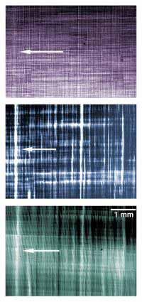
X-ray topographs of three different strata of a strained-silicon wafer show close correspondence in defects from the base silicon layer (top) through the final strained-silicon layer (bottom). Color has been added for contrast, one particular defect area is highlighted. Credit: Courtesy National Institute of Standards and Technology
Strained silicon is a new, rapidly developing material for building enhanced-performance silicon-based transistors. Introducing a slight tensile strain in the lattice of the silicon crystal dramatically improves the mobility of charges in the crystal, enabling faster, higher-performance devices. The strain is achieved by first growing a relatively thick crystalline layer of silicon-germanium (SiGe) on the normal silicon substrate wafer, and then growing a thin film of pure silicon on top. The difference in lattice spacing between pure silicon and SiGe creates the desired strain, but also creates occasional defects in the crystal that degrade performance. The problem is particularly bad when the defects cluster together in so-called “pile-ups.”
One of the best methods for studying crystal defects is to observe the image of X-rays diffracted from the crystal planes, a technique called X-ray topography. Until now, however, it's been impossible to study the interaction of defects in the multiple layers of these complex Si – SiGe – Si wafers. In a recent paper in Applied Physics Letters,* researchers from NIST and AmberWave Systems Corporation (Salem, N.H.) detail a high-resolution form of X-ray topography that can distinguish individual crystal defects layer by layer. The technique combines an extremely low-angle incident X-ray beam (“glancing incidence”) to increase the signal from one layer over another and the use of highly monochromatic X-rays tuned to separate the contributions from each layer based on their different lattice spacings.
Their results show that crystal defects initially created at the interface between the silicon wafer and the SiGe layer become “templates” that propagate through that layer and create matching defects in the strained-silicon top layer. These defects, in turn, are notably persistent, remaining in the strained-silicon even through later processing that includes stripping the layer off, bonding it to an oxidized silicon wafer, and annealing it to create strained-silicon-on-insulator (SSOI) substrates.
Media Contact
More Information:
http://www.nist.govAll latest news from the category: Physics and Astronomy
This area deals with the fundamental laws and building blocks of nature and how they interact, the properties and the behavior of matter, and research into space and time and their structures.
innovations-report provides in-depth reports and articles on subjects such as astrophysics, laser technologies, nuclear, quantum, particle and solid-state physics, nanotechnologies, planetary research and findings (Mars, Venus) and developments related to the Hubble Telescope.


Newest articles
Red light therapy for repairing spinal cord injury passes milestone
Patients with spinal cord injury (SCI) could benefit from a future treatment to repair nerve connections using red and near-infrared light. The method, invented by scientists at the University of…
Insect research is revolutionized by technology
New technologies can revolutionise insect research and environmental monitoring. By using DNA, images, sounds and flight patterns analysed by AI, it’s possible to gain new insights into the world of…

X-ray satellite XMM-newton sees ‘space clover’ in a new light
Astronomers have discovered enormous circular radio features of unknown origin around some galaxies. Now, new observations of one dubbed the Cloverleaf suggest it was created by clashing groups of galaxies….

