Large area transistors get helping hand from quantum effects
The unexpected superior switching performance (low leakage current, and steep sub-threshold slope) shown experimentally and analysed theoretically, demonstrate hitherto unexplored routes for improvements for transistors based on disordered silicon films.
By making the conduction channel in these disordered transistors very thin, the team has shown this technology will enable the design of low power memory for large area electronics based on a low-cost industry standard material processing route.
In the most recent investigations, the current of the devices, is found to be percolation governed when the channel is thinner than 3.0 nm due to strong quantum confinement induced potential variations over the active channel region. It is shown that the device channel width must be at least 0.3 µm to avoid percolative “pinch off” for 0.5 µm channel length devices. Theoretical analysis performed on the devices agrees well with the experimental data and provides important guidelines to model and optimize the devices for circuit design.
Dr Xiaojun Guo, one of the lead investigators, comments: “The nano-structure silicon thin-film transistors are very promising for design of low power electronics. However, carrier transport in such devices is very complicated, and results in electrical characteristics that may not be described by conventional field effect transistor (FET) models. This work reveals the key physical properties of the devices, which will help to further optimize and model the devices for circuit design”.
Professor Ravi Silva, Director of the Advanced Technology Institute adds: “This study is a prime example of how leading silicon technologies entrenched in industry can find alternative routes to improve on performance in device characteristics by clever design. The role that funding organizations such as EPSRC play in supporting this type of applied research is invaluable to the community and most importantly to industry”.
The results are published in Applied Physics Letters 93 (2008) 042105.
Reference:
X. Guo, S.R.P. Silva, T. Ishii, “Current percolation in ultrathin channel nanocrystalline silicon transistors”, Applied Physics Letters 93, (2008) 042105.
Media Contact
More Information:
http://www.surrey.ac.ukAll latest news from the category: Physics and Astronomy
This area deals with the fundamental laws and building blocks of nature and how they interact, the properties and the behavior of matter, and research into space and time and their structures.
innovations-report provides in-depth reports and articles on subjects such as astrophysics, laser technologies, nuclear, quantum, particle and solid-state physics, nanotechnologies, planetary research and findings (Mars, Venus) and developments related to the Hubble Telescope.


Newest articles
Economies take off with new airports
A global study by an SUTD researcher in collaboration with scientists from Japan explores the economic benefits of airport investment in emerging economies using nighttime satellite imagery. Be it for…
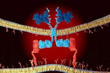
CAR T–cell immunotherapy targets
Pan-cancer analysis uncovers a new class of promising CAR T–cell immunotherapy targets. Scientists at St. Jude Children’s Research Hospital found 156 potential CAR targets across the brain and solid tumors,…
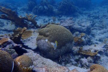
Stony coral tissue loss disease
… is shifting the ecological balance of Caribbean reefs. The outbreak of a deadly disease called stony coral tissue loss disease is destroying susceptible species of coral in the Caribbean…

