Self-assembled nanostructures enable a low-power phase-change memory for mobile electronic devices
Flash memory is a dominant technology in this field, but its slow writing and erasing speed has led to extensive research into a next-generation nonvolatile memory called Phase-Change Random Access Memory (PRAM), as PRAM's operating speed is 1,000 times faster than that of flash memory.
PRAM uses reversible phase changes between the crystalline (low resistance) and amorphous (high resistance) state of chalcogenide materials, which corresponds to the data “0” and “1,” respectively. Although PRAM has been partially commercialized up to 512 Mb by Samsung Electronics Co., Ltd., its writing current should be decreased by at least one-third of its present level for the mass production of mobile electronics applications.
A team of Professors Keon Jae Lee and Yeon Sik Jung in the Department of Materials Science and Engineering at KAIST has developed phase-change memory with low power consumption (below 1/20th of its present level) by employing self-assembled block copolymer (BCP) silica nanostructures. Their work was published under the title “Self-Assembled Incorporation of Modulated Block Copolymer Nanostructures in Phase-Change Memory for Switching Power Reduction” in the March issue of ACS Nano, a monthly peer-reviewed scientific journal.
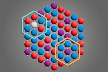
BCP is the mixture of two different polymer materials, which can easily create self-ordered arrays of sub-20 nm features through simple spin-coating and plasma treatments. PRAM can lower switching power consumption by making the contact area smaller between the heating layer and phase change materials. Professor Lee's team successfully decreased the size of the contact area and the level of power consumption by incorporating self-assembled silica nanostructures on top of conventional phase-change materials. Interestingly, these self-assembled nanomaterials are able to reduce power much more than expected with localized nano-switching mechanisms.
Professor Keun-Jae Lee said, “This is a very good example that self-assembled, bottom-up nanotechnology can actually enhance the performance of electronic devices. We also achieved a significant power reduction through a simple process that is compatible with conventional device structures and existing lithography tools.”
The research team is currently investigating self-assembled BCP applications for resistive random access memory and flexible electronic devices.
Media Contact
More Information:
http://www.kaist.ac.krAll latest news from the category: Materials Sciences
Materials management deals with the research, development, manufacturing and processing of raw and industrial materials. Key aspects here are biological and medical issues, which play an increasingly important role in this field.
innovations-report offers in-depth articles related to the development and application of materials and the structure and properties of new materials.


Newest articles
Microscopic basis of a new form of quantum magnetism
Not all magnets are the same. When we think of magnetism, we often think of magnets that stick to a refrigerator’s door. For these types of magnets, the electronic interactions…

An epigenome editing toolkit to dissect the mechanisms of gene regulation
A study from the Hackett group at EMBL Rome led to the development of a powerful epigenetic editing technology, which unlocks the ability to precisely program chromatin modifications. Understanding how…
NASA selects UF mission to better track the Earth’s water and ice
NASA has selected a team of University of Florida aerospace engineers to pursue a groundbreaking $12 million mission aimed at improving the way we track changes in Earth’s structures, such…

