A Novel Energy-Band Model for Semiconducting Spintronics Material Gallium Manganese Arsenide
The University of Tokyo announced on February 7, 2011 that Professor M. Tanaka and his colleagues have succeeded in determining the Fermi level position and band structure in semiconducting spintronics material gallium manganese arsenide (GaMnAs) by a unique method combining a precise etching technique and resonant tunneling spectroscopy. Details were presented in Nature Physics*.
A ferromagnetic semiconductor is a basic material for spintronics which utilizes “electron spin” to realize new functional devices. Although GaMnAs is such a typical ferromagnetic material, its band structure has been controversial. Prevalent model assumes a valence band merged with an impurity band due to Mn atoms, with the Fermi level located inside the band and holes contribute to electrical conduction. However, optical study has shown that the Fermi level is located outside of valence band.
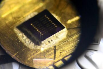
In this work, layers of 100nm thick beryllium-doped gallium arsenide (GaAs), 5nm thick aluminium arsenide tunnel barrier and GaMnAs were grown successively on a (001) GaAs substrate. The GaMnAs layer is etched to various thickness of 4.6-22nm to make quantum wells of different thickness between the surface and the tunnel barrier. Resonant tunneling spectroscopy, applied to a variety of surface GaMnAs layers, can elucidate the valence-band (VB) picture of GaMnAs. The VB structure of GaAs is almost perfectly maintained and does not merge with the impurity band for any of the GaMnAs samples, with manganese concentrations ranging from 6 to 15%. Furthermore, the exchange splitting of the VB is found to be very small (only several milli-eV), even in GaMnAs with a high Curie temperature (154K).
Researchers suggest that their findings shed light on the precise mechanism behind ferromagnetism in GaMnAs; a subject that has been debated for more than a decade.
Journal information
*Shinobu Ohya, Kenta Takata & Masaaki Tanaka, “Nearly non-magnetic valence band of the ferromagnetic semiconductor GaMnAs”, Nature Physics (2011) DOI: doi:10.1038/nphys1905 Published online 06 February 2011.
Media Contact
All latest news from the category: Materials Sciences
Materials management deals with the research, development, manufacturing and processing of raw and industrial materials. Key aspects here are biological and medical issues, which play an increasingly important role in this field.
innovations-report offers in-depth articles related to the development and application of materials and the structure and properties of new materials.


Newest articles

Sea slugs inspire highly stretchable biomedical sensor
USC Viterbi School of Engineering researcher Hangbo Zhao presents findings on highly stretchable and customizable microneedles for application in fields including neuroscience, tissue engineering, and wearable bioelectronics. The revolution in…

Twisting and binding matter waves with photons in a cavity
Precisely measuring the energy states of individual atoms has been a historical challenge for physicists due to atomic recoil. When an atom interacts with a photon, the atom “recoils” in…
Nanotubes, nanoparticles, and antibodies detect tiny amounts of fentanyl
New sensor is six orders of magnitude more sensitive than the next best thing. A research team at Pitt led by Alexander Star, a chemistry professor in the Kenneth P. Dietrich…

