molecular-beam epitaxy
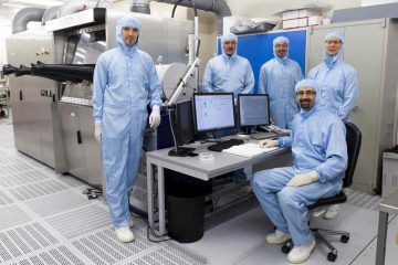
World’s first production of aluminum scandium nitride via MOCVD
Transistors based on AlScN are promising for various industrial applications, such as data transfer, satellite communication, radar systems or autonomous…
Shell increases versatility of nanowires
Nanowires are extremely versatile. The tiny elements can be used for miniaturized photonic and electronic components in nanotechnology. Applications include…
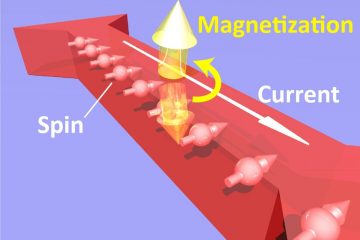
Small currents for big gains in spintronics
UTokyo researchers have created an electronic component that demonstrates functions and abilities important to future generations of computational logic and…
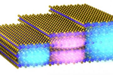
Nano-imaging of intersubband transitions in few-layer 2D materials
Quantum wells of the highest quality are typically fabricated by molecular beam epitaxy (sequential growth of crystalline layers), which is a well-established…
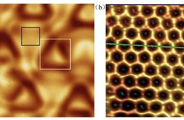
Boron can form a purely honeycomb, graphene-like 2-D structure
An intriguing question is whether it is possible to prepare a borophene monolayer with a pure honeycomb lattice. Honeycomb borophene will naturally host Dirac…
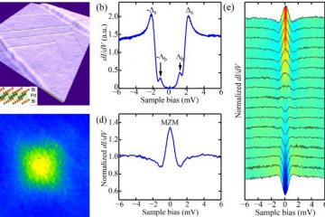
Physicists demonstrate topological superconductivity on palladium dibismuthides
A topological superconductor is superconducting inside the bulk like usual superconductors, while on the boundary/surface it harbors the long-sought Majorana…