World’s first production of aluminum scandium nitride via MOCVD
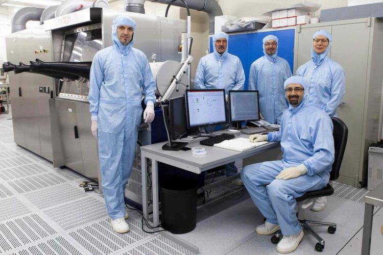
Scientists at Fraunhofer IAF are the world’s first to produce aluminum scandium nitride (AlScN) via metal-organic chemical vapor deposition (MOCVD). Fraunhofer IAF
Transistors based on AlScN are promising for various industrial applications, such as data transfer, satellite communication, radar systems or autonomous driving, especially since current devices based on silicon (Si) are reaching their physical limit in these applications.
One reason for this is the size of Si devices, which cannot be reduced any more according to the current state of research. If the ever-increasing amounts of data had to be processed with the current Si technology, the server rooms would occupy such a large area that it would be economically and ecologically unstainable.
So-called HEMTs (high electron mobility transistors) surpass the possibilities of Si devices by far. The key to the success of HEMT structures lies in the materials they are based on. AlScN has exceptional properties, allowing higher carrier concentrations than other materials. In the future, significantly more powerful and efficient HEMTs will be realized based on AlScN.
Previous manufacturing processes have failed due to quality and productivity
The production of AlScN involves fundamental challenges. The state-of-the-art production process grows AlScN layers via sputtering. Unfortunately, the quality of these layers is insufficient for electronic applications such as LEDs and high-power transistors. An alternative method is to produce AlScN via molecular beam epitaxy (MBE). With this process, high amounts of scandium can be incorporated in the compound. The quality is also sufficient for the production of microelectronic devices. However, the procedure is very complex and the productivity too low for industrial scale productions.
Metal-organic chemical vapor deposition promises industrial-grade production
The production of AlScN via MOCVD promises not only the necessary quality, but also sufficient productivity for industrial applications. “We knew that previous attempts by other scientists to produce gallium scandium nitride via MOCVD had failed. We also know that many scientists all over the world are working to develop AlScN transistors, but no one before us has succeeded in doing it by using MOCVD, even though it is a very promising approach for industry”, explains Dr Stefano Leone, group leader at Fraunhofer IAF.
During the MOCVD procedure gases are guided across a heated wafer. Through the heat exposure distinct molecules are released from the gas and integrated into the crystalline structure of the wafer. The crystal structure can be precisely adjusted by regulating the gas flow, temperature and pressure. Furthermore, the quick change of gas allows to grow different material layers on top of each other.
Fraunhofer IAF achieves novelty
The challenge for the researchers at Fraunhofer IAF: there is no gas source for scandium. The molecules (precursors) for scandium are very large and difficult to bring into the gas phase. “We studied the best possible precursor for scandium and planned adjustments of our MOCVD reactor for the necessary procedure. We did a lot of research and had numerous discussions until we developed a setup that we are now even patenting. We have now succeeded in growing AlScN layers via MOCVD with a very high crystal quality and the right amount of scandium in order to develop the next generation of power transistors”, says Leone, pleased with the achievement. The MOCVD system at Fraunhofer IAF has been modified by the research group to enable a high-quality and reproducible AlScN production process.
First AlScN layers for transistors from the MOCVD
After the successful deposition of AlScN in the MOCVD system, the first AlScN layers for transistors were produced. The layers already reach promising results with a sheet resistance of ~200 ohm/sq., a mobility of ~600 cm²/Vs and a charge carrier density of ~4,0 x 10¹³ cm⁻². The current goal of the scientists is to reduce the sheet resistance and to further increase the mobility and material quality. This will improve the performance of future transistors and Fraunhofer IAF will take a significant step towards its goal of providing AlScN HEMTs for industrial power electronic applications.
https://www.iaf.fraunhofer.de/en/media-library/press-releases/aluminum-scandium-…
Media Contact
All latest news from the category: Physics and Astronomy
This area deals with the fundamental laws and building blocks of nature and how they interact, the properties and the behavior of matter, and research into space and time and their structures.
innovations-report provides in-depth reports and articles on subjects such as astrophysics, laser technologies, nuclear, quantum, particle and solid-state physics, nanotechnologies, planetary research and findings (Mars, Venus) and developments related to the Hubble Telescope.


Newest articles

Silicon Carbide Innovation Alliance to drive industrial-scale semiconductor work
Known for its ability to withstand extreme environments and high voltages, silicon carbide (SiC) is a semiconducting material made up of silicon and carbon atoms arranged into crystals that is…

New SPECT/CT technique shows impressive biomarker identification
…offers increased access for prostate cancer patients. A novel SPECT/CT acquisition method can accurately detect radiopharmaceutical biodistribution in a convenient manner for prostate cancer patients, opening the door for more…

How 3D printers can give robots a soft touch
Soft skin coverings and touch sensors have emerged as a promising feature for robots that are both safer and more intuitive for human interaction, but they are expensive and difficult…

