


Feeding 9 Billion: Innovations in Agricultural Modeling
A review led by KAUST researchers sheds light on the strengths and weaknesses of different buffer materials used in optoelectronic devices.
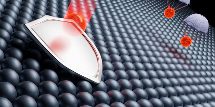
Credit: © 2021 KAUST; Hassan Tahini
Crucial in the design of any semiconductor device is how to inject and extract an electrical current, and now a KAUST-led team has reviewed ways to do this without damage to the device.
A basic metal-semiconductor interface can create a potential energy barrier to the efficient flow of electrons, depending on the electronic properties of the two materials. It is vital to make a careful choice of contact material and the process by which this material is deposited onto the semiconductor. These design considerations are more complicated for optoelectronic components such as light-emitting diodes (LEDs), photodetectors and solar cells because these devices require a transparent contact material to allow light in or out.
Erkan Aydin and Stefaan De Wolf from the KAUST Solar Center, along with co-authors from Turkey, the Netherlands and Spain, have presented an overview for the process to stop damage occurring on devices during the creation of transparent electrodes, particularly for a technique known as sputtering.
Sputtering works by placing the target semiconductor into a vacuum chamber and surrounding it in a plasma. When an electric field is created between the target and the cathode made of the material to be sputtered, the fast-moving plasma ions transfer atoms/molecules from one to the other.
This technique is particularly useful for creating low resistivity and high transparency thin films of transparent conductive oxides (TCO), such as indium tin oxide (ITO).
However, the high kinetic energy of the ions can damage the semiconductor target. This degradation is severe enough to be seen using optical and electron microscopes, and leads to, for example, poorer device operation, lower maximum power output in solar cells and higher leakage current in LEDs.
“This is a common problem for many optoelectronic devices, but there is no universalized solution to mitigate it,” says Aydin.
Aydin and colleagues reviewed strategies for mitigating this damage, in particular using a buffer layer between the semiconductor and the electrode. “As a rule of thumb, buffer layers should be able to tolerate the particle damage during the sputtering process, while also functioning electronically and being optically transparent,” explains Aydin.
The co-authors summarize the strengths and weaknesses of different buffer materials and their suitability for different optoelectronic applications. They also compare numerous techniques for creating the buffer and give an overview for developing damage-free deposition of TCOs on optoelectronic devices in future.
“With this comprehensive review, we elaborate the problem from multiple aspects and give the readers a basic understanding of the issue and offer some cross-disciplinary learnings,” says Aydin.
Journal: Matter
DOI: https://doi.org/10.1016/j.matt.2021.09.021
Article Title: Sputtered transparent electrodes for optoelectronic devices: Induced damage and mitigation strategies
Article Publication Date: 3-Nov-2021

![[Figure 1] Schematic of next-generation CNT-PANI composite fiber supercapacitor and comparison graph with recent results](https://www.innovations-report.com/wp-content/uploads/2025/05/KIST_leads_next-generation_energy_storage_technolo_1746783279-e1746784635527-362x245.jpg)
Developing next-generation energy storage technologies that enable high power and capacity simultaneously A research team led by Dr. Bon-Cheol Ku and Dr. Seo Gyun Kim of the Carbon Composite Materials Research Center at the Korea Institute of Science and Technology (KIST) and Professor Yuanzhe Piao of Seoul National University (SNU) has developed a high-performance supercapacitor that is expected to become the next generation of energy storage devices. The technology developed by the researchers overcomes the limitations of existing supercapacitors by…

Greater coordination among states could save the region up to $3.25 billion per year in energy system costs A new study led by researchers at the University of California San Diego offers a first-of-its-kind look at how deeper coordination among Western U.S. states could lower the cost of decarbonizing the electric grid—and speed up the clean energy transition. Published in the journal Nature Communications, the paper models how 11 Western states—including California, Arizona, and New Mexico—might build out clean energy…

Power inverters are the beating heart in the drive train of modern electric cars. They turn the electrical energy from the batteries into something that engines can actually use. Fraunhofer IZM has now redefined what this key component is possible of doing: Using the newest developments in power electronics, the „Dauerpower“ inverter was born that can handle enormous amounts of power with low inductance and in a tiny body – with peak efficiency measured at 98.7%. Let’s roll! Modern electric…

Researchers developed a compact, solid-state laser system that generates 193-nm coherent light — the first 193-nm vortex beam — promising significant advancements in semiconductor lithography and other high-tech applications Deep ultraviolet (DUV) lasers, known for their high photon energy and short wavelengths, are essential in various fields such as semiconductor lithography, high-resolution spectroscopy, precision material processing, and quantum technology. These lasers offer increased coherence and reduced power consumption compared to excimer or gas discharge lasers, enabling the development of more…


