


Feeding 9 Billion: Innovations in Agricultural Modeling
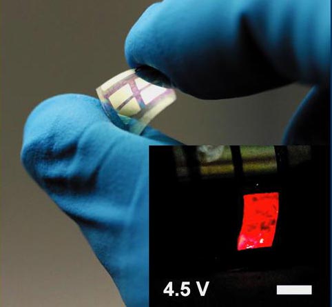
Foil with 1 cm edge length, containing four emitter elements. The insert shows one of them in operation. The scalebar is 2 mm.
Andrzejewski et al., Advanced Optical Materials 2020, 2000694, Published by Wiley-VCH, Weinheim
If 80,000 of them were piled on top of each other, the stack would only be as high as a flat sheet of paper. Scientists from the Center for Nanointegration (CENIDE) at the University of Duisburg-Essen (UDE) and cooperation partners have developed a layer of tungsten disulfide that is just as thin as three atomic layers – and it is luminous, flexible and also withstands external influences. Several square centimeters of this layer have already been embedded in structural components, but the manufacturing process is scalable beyond that, the trade journal Advanced Optical Materials reports.
The wafer-thin luminescent layer grows on a sapphire base, is then carefully removed with the aid of a lacquer and transferred to the carrier film. The lacquer is then dissolved. In broad terms, this is the manufacturing process the project partners from UDE, RWTH Aachen University and AIXTRON used to develop entire devices from the two-dimensional material. The method can be scaled to much larger areas using the same material and the same device architecture, and this is what makes it interesting from an industrial point of view.
Change the Bending to Change the Light
Led by UDE’s Professor Gerd Bacher, lighting elements were created that combine the advantages of different component concepts: The inorganic tungsten disulfide layer is less susceptible to harmful environmental influences such as oxygen or moisture and is also long-term stable. Due to the flexible design, the structure adapts to any shape. But the flexibility has even another advantage: if the film is bent, the crystal lattice of the luminous layer is distorted and the wavelength of the emitted light – and thus the color of the light – changes. Although this difference is not visible to the naked eye, it is easy to detect with measuring instruments.
“This is what makes the elements interesting as sensors, for instance,” explains Dr. Tilmar Kümmell from the Bacher working group. “We think they could be used to detect deformation or distortions.” On the other hand, the precise bending of the film would also make it possible to select a specific wavelength for the emitted light.
Editor: Birte Vierjahn, +49 203/37 9-8176, birte.vierjahn@uni-due.de
Dr. Tilmar Kümmell, Electronic Materials and Nanostructures, +49 203/37 9-3403, tilmar.kuemmell@uni-due.de
D. Andrzejewski, R. Oliver, Y. Beckmann, A. Grundmann, M. Heuken, H. Kalisch, A. Vescan, T. Kümmell, G. Bacher
„Flexible large-area light-emitting devices based on WS2 monolayers“
Advanced Optical Materials 2020, 2000694
https://doi.org/10.1002/adom.202000694
http://www.uni-duisburg-essen.de/

![[Figure 1] Schematic of next-generation CNT-PANI composite fiber supercapacitor and comparison graph with recent results](https://www.innovations-report.com/wp-content/uploads/2025/05/KIST_leads_next-generation_energy_storage_technolo_1746783279-e1746784635527-362x245.jpg)
Developing next-generation energy storage technologies that enable high power and capacity simultaneously A research team led by Dr. Bon-Cheol Ku and Dr. Seo Gyun Kim of the Carbon Composite Materials Research Center at the Korea Institute of Science and Technology (KIST) and Professor Yuanzhe Piao of Seoul National University (SNU) has developed a high-performance supercapacitor that is expected to become the next generation of energy storage devices. The technology developed by the researchers overcomes the limitations of existing supercapacitors by…

Greater coordination among states could save the region up to $3.25 billion per year in energy system costs A new study led by researchers at the University of California San Diego offers a first-of-its-kind look at how deeper coordination among Western U.S. states could lower the cost of decarbonizing the electric grid—and speed up the clean energy transition. Published in the journal Nature Communications, the paper models how 11 Western states—including California, Arizona, and New Mexico—might build out clean energy…

Power inverters are the beating heart in the drive train of modern electric cars. They turn the electrical energy from the batteries into something that engines can actually use. Fraunhofer IZM has now redefined what this key component is possible of doing: Using the newest developments in power electronics, the „Dauerpower“ inverter was born that can handle enormous amounts of power with low inductance and in a tiny body – with peak efficiency measured at 98.7%. Let’s roll! Modern electric…

Researchers developed a compact, solid-state laser system that generates 193-nm coherent light — the first 193-nm vortex beam — promising significant advancements in semiconductor lithography and other high-tech applications Deep ultraviolet (DUV) lasers, known for their high photon energy and short wavelengths, are essential in various fields such as semiconductor lithography, high-resolution spectroscopy, precision material processing, and quantum technology. These lasers offer increased coherence and reduced power consumption compared to excimer or gas discharge lasers, enabling the development of more…


