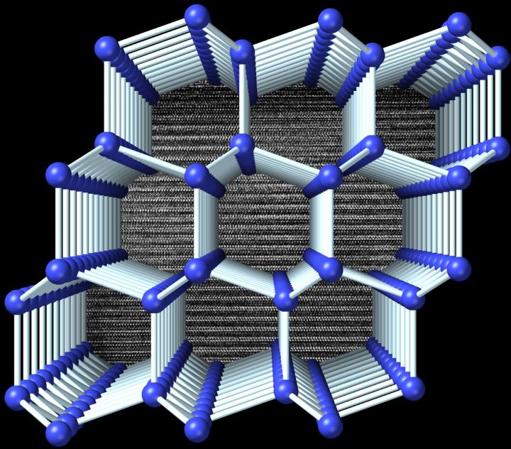

Visualization of the structure of 4H-Si viewed perpendicular to the hexagonal axis. A transmission electron micrograph showing the stacking sequence is displayed in the background.
Image courtesy of Thomas Shiell and Timothy Strobel
Novel crystalline form of silicon could potentially be used to create next-generation electronic and energy devices.
A team led by Carnegie’s Thomas Shiell and Timothy Strobel developed a new method for synthesizing a novel crystalline form of silicon with a hexagonal structure that could potentially be used to create next-generation electronic and energy devices with enhanced properties that exceed those of the “normal” cubic form of silicon used today.
Their work is published in Physical Review Letters.
Silicon plays an outsized role in human life. It is the second most abundant element in the Earth’s crust. When mixed with other elements, it is essential for many construction and infrastructure projects. And in pure elemental form, it is crucial enough to computing that the longstanding technological hub of the U.S.–California’s Silicon Valley–was nicknamed in honor of it.
Like all elements, silicon can take different crystalline forms, called allotropes, in the same way that soft graphite and super-hard diamond are both forms of carbon. The form of silicon most commonly used in electronic devices, including computers and solar panels, has the same structure as diamond. Despite its ubiquity, this form of silicon is not actually fully optimized for next-generation applications, including high-performance transistors and some photovoltaic devices.
While many different silicon allotropes with enhanced physical properties are theoretically possible, only a handful exist in practice given the lack of known synthetic pathways that are currently accessible.
Strobel’s lab had previously developed a revolutionary new form of silicon, called Si24, which has an open framework composed of a series of one-dimensional channels. In this new work, Shiell and Strobel led a team that used Si24 as the starting point in a multi-stage synthesis pathway that resulted in highly oriented crystals in a form called 4H-silicon, named for its four repeating layers in a hexagonal structure.
“Interest in hexagonal silicon dates back to the 1960s, because of the possibility of tunable electronic properties, which could enhance performance beyond the cubic form” Strobel explained.
Hexagonal forms of silicon have been synthesized previously, but only through the deposition of thin films or as nanocrystals that coexist with disordered material. The newly demonstrated Si24 pathway produces the first high-quality, bulk crystals that serve as the basis for future research activities.
Using the advanced computing tool called PALLAS, which was previously developed by members of the team to predict structural transition pathways–like how water becomes steam when heated or ice when frozen–the group was able to understand the transition mechanism from Si24 to 4H-Si, and the structural relationship that allows the preservation of highly oriented product crystals.
“In addition to expanding our fundamental control over the synthesis of novel structures, the discovery of bulk 4H-silicon crystals opens the door to exciting future research prospects for tuning the optical and electronic properties through strain engineering and elemental substitution,” Shiell said. “We could potentially use this method to create seed crystals to grow large volumes of the 4H structure with properties that potentially exceed those of diamond silicon.”
###
Carnegie’s Li Zhu was also a member of the research team, along with Brenton Cook and Dougal McCulloch of RMIT University and Jodie Bradby of The Australian National University.
This work was supported by the National Science Foundation, Division of Materials Research.
Portions of this work were performed at HPCAT (Sector 16), Advanced Photon Source (APS), Argonne National Laboratory. HPCAT operations are supported by DOE-NNSA’s Office of Experimental Sciences. The Advanced Photon Source is a U.S. Department of Energy (DOE) Office of Science User Facility operated for the DOE Office of Science by Argonne National Laboratory.


