


Feeding 9 Billion: Innovations in Agricultural Modeling
A chip-scale metalens array makes this microscope system ultracompact.
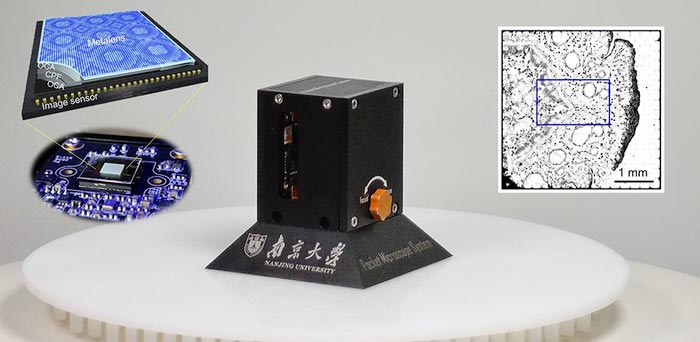
Credit: Tao Li, Nanjing University
A newly developed polarizer-embedded metalens enables a compact, portable microscope system that efficiently obtains wide-field, noise-free, high-resolution images.
The microscope effectively expands human eyesight to microworld. It supports wide applications in scientific research, biomedical diagnosis, industry, and beyond. The ultimate goal is superresolution, yet along the way researchers are working to achieve compact, miniature devices with comprehensive performance for wide field-of-view (FOV), large depth-of-field (DOF), and high throughput.
Traditional optical microscopes are based on refractive optical elements, which are usually bulky and heavy with limitations in FOV and DOF, though they have been substantially developed. Flat diffractive lenses seemed to offer a possible solution to miniaturize imaging systems, but they achieve low efficiency and poor imaging quality. Recent lensless imaging technology considerably revolutionizes imaging technology and enables highly compact imaging devices, but it strongly depends on postprocessing computation, which is resource-intensive and risks distortion.
Metalens technology opens a new way to achieve ultracompact and lightweight optical imaging systems. A metalens is a kind of metasurface composed of subwavelength units with powerful capability for manipulating light. An innovative polarization multiplexed metalens array (based on silicon nanoposts) was proposed to realize a compact and wide-field microscope that breaks conventional FOV constraints, but the imaging quality is relatively poor due to its low efficiency with background noise, and the overall FOV is still smaller than that of traditional microscope with the same resolution.
Significantly improved imaging quality is now possible with higher-resolution imaging, thanks to researchers from Nanjing University who developed a polarizer-embedded metalens imaging device (PMID). As reported in Advanced Photonics, the PMID is implemented based on a silicon nitride metasurface mounted on a CMOS image sensor with a fixed circular-polarization filter inserted between the two. It eliminates background noises, and even enables zoom-in imaging.
The system is based on a special co-and-cross-multiplexed metalens array and embedded polarizer. By integrating them to a chip-scale CMOS sensor, the researchers successfully developed a high-quality wide FOV and large DOF microscopy technique. Significantly high performances are achieved, with a 4×4-mm2 FOV, a 1.74-μm resolution (limited by the CMOS pixel size), and a ~200-μm DOF (450-510-nm wavelength range). This FOV is around 5 to 7 times that of a traditional microscope with the same resolution. The team demonstrated the outstanding microscopy performance by imaging a large number of bio-specimens.
According to senior author Tao Li, principal investigator at Nanjing University’s National Laboratory of Solid-State Microstructures, “To the best of our knowledge, this is the first time a metalens imager has accessed a larger FOV than a traditional microscope with similar imaging quality. By sweeping the illumination wavelength, the device is able to achieve large depth-of-field imaging simultaneously, thanks to the large dispersive nature of the metalens.” Li further remarks, “This chip-scale PMID enables the implementation of miniaturized portable microscope system, with a thousand-fold reduction in volume and weight compared to a traditional microscope.”
This chip-scale microscope promises to revolutionize traditional optical devices, presenting a new horizon of ultracompact imaging devices powered by metatechnology.
Read the Gold Open Access article by Xin Ye et al., “Chip-scale metalens microscope for wide-field and depth-of-field imaging,” Adv. Photon. 4(4), 046006 (2022), doi 10.1117/1.AP.4.4.046006.
Journal: Advanced Photonics
DOI: 10.1117/1.AP.4.4.046006
Article Title: Chip-scale metalens microscope for wide-field and depth-of-field imaging
Article Publication Date: 27-Jul-2022
Media Contact
Daneet Steffens
SPIE–International Society for Optics and Photonics
daneets@spie.org
Office: 360-685-5478


Astronomers have created a galactic masterpiece: an ultra-detailed image that reveals previously unseen features in the Sculptor Galaxy. Using the European Southern Observatory’s Very Large Telescope (ESO’s VLT), they observed this nearby galaxy in thousands of colours simultaneously. By capturing vast amounts of data at every single location, they created a galaxy-wide snapshot of the lives of stars within Sculptor. “Galaxies are incredibly complex systems that we are still struggling to understand,” says ESO researcher Enrico Congiu, who led a…

NASA spacecraft make progress in final commissioning, preliminary science operations SAN ANTONIO — June 10, 2025 — Southwest Research Institute’s Dr. Craig DeForest discussed the latest accomplishments of NASA’s PUNCH (Polarimeter to Unify the Corona and Heliosphere) mission during a media event at the 246th American Astronomical Society meeting in Anchorage, Alaska. As the spacecraft constellation completes commissioning, early PUNCH data showed coronal mass ejections, or CMEs, as they erupted from the Sun and traveled across the inner solar system….

Using advanced computational modelling, a research team led by the University of Oxford, working in partnership with the Instituto Superior Técnico in the University of Lisbon, has achieved the first-ever real-time, three-dimensional simulations of how intense laser beams alter the ‘quantum vacuum’—a state once assumed to be empty, but which quantum physics predicts is full of virtual electron-positron pairs. Excitingly, these simulations recreate a bizarre phenomenon predicted by quantum physics, known as vacuum four-wave mixing. This states that the combined…

An international team of astronomers, including researchers from the University of Liège and collaborators in UK, Chile, the USA, and Europe, has discovered a giant planet orbiting the smallest known star to host such a companion The host star, TOI-6894, is a red dwarf with only 20% the mass of the Sun, typical of the most common stars in our galaxy. Until now, such low-mass stars were not thought capable of forming or retaining giant planets. But as published today…


