


Feeding 9 Billion: Innovations in Agricultural Modeling
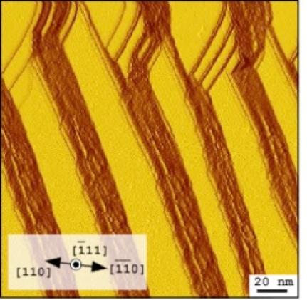
Spatial-derivative STM images with 200x200 nm^2 at Vs = +1.5 V. Flat terraces become brighter and edges darker. The downstairs direction runs from left ((110) top-surface) to right ((-1-10) back-surface).
Credit: Osaka University
A research collaboration between Osaka University and the Nara Institute of Science and Technology for the first time used scanning tunneling microscopy (STM) to create images of atomically flat side-surfaces of 3D silicon crystals.
This work helps semiconductor manufacturers continue to innovate while producing smaller, faster, and more energy-efficient computer chips for computers and smartphones.
Our computers and smartphones each are loaded with millions of tiny transistors. The processing speed of these devices has increased dramatically over time as the number of transistors that can fit on a single computer chip continues to increase.
Based on Moore's Law, the number of transistors per chip will double about every 2 years, and in this area it seems to be holding up. To keep up this pace of rapid innovation, computer manufacturers are continually on the lookout for new methods to make each transistor ever smaller.
Current microprocessors are made by adding patterns of circuits to flat silicon wafers. A novel way to cram more transistors in the same space is to fabricate 3D-structures. Fin-type field effect transistors (FETs) are named as such because they have fin-like silicon structures that extend into the air, off the surface of the chip.
However, this new method requires a silicon crystal with a perfectly flat top and side-surfaces, instead of just the top surface, as with current devices. Designing the next generation of chips will require new knowledge of the atomic structures of the side-surfaces.
Now, researchers at Osaka University and the Nara Institute of Science and Technology report that they have used STM to image the side-surface of a silicon crystal for the first time. STM is a powerful technique that allows the locations of the individual silicon atoms to be seen.
By passing a sharp tip very close to the sample, electrons can jump across the gap and create an electrical current. The microscope monitored this current, and determined the location of the atoms in the sample.
“Our study is a big first step toward the atomically resolved evaluation of transistors designed to have 3D-shapes,” study coauthor Azusa Hattori says.
To make the side-surfaces as smooth as possible, the researchers first treated the crystals with a process called reactive ion etching. Coauthor Hidekazu Tanaka says, “Our ability to directly look at the side-surfaces using STM proves that we can make artificial 3D structures with near-perfect atomic surface ordering.”


A new quantum random number generator is almost 1000 times faster than other generators and much smaller, promising to change data management and cybersecurity in several industries including health, finance, and defense A joint team of researchers led by scientists at King Abdullah University of Science and Technology (KAUST) and King Abdulaziz City for Science and Technology (KACST) has reported the fastest quantum random number generator (QRNG) to date based on international benchmarks. The QRNG, which passed the required randomness…

Very secure and highly efficient: encryption and decryption with luminescent perovskites To guarantee high data security, encryption must be unbreakable while the data remains rapidly and easily readable. A novel strategy for optical encryption/decryption of information has now been introduced in the journal Angewandte Chemie by a Chinese research team. It is based on compounds with carefully modulated luminescent properties that change in response to external stimuli. The compounds are hybrid two-dimensional organic-inorganic metal-halide perovskites, whose structure consists of inorganic…

Researchers at the University of Utah’s Department of Psychiatry and Huntsman Mental Health Institute today published a paper introducing RiskPath, an open source software toolkit that uses Explainable Artificial Intelligence (XAI) to predict whether individuals will develop progressive and chronic diseases years before symptoms appear, potentially transforming how preventive healthcare is delivered. XAI is an artificial intelligence system that can explain complex decisions in ways humans can understand. The new technology represents a significant advancement in disease prediction and prevention…

Researchers train AI to predict if and why proteins form sticky clumps, a mechanism linked to 50 human diseases affecting half a billion people An AI tool has made a step forward in translating the language proteins use to dictate whether they form sticky clumps similar to those linked to Alzheimer’s Disease and around fifty other types of human disease. In a departure from typical “black-box” AI models, the new tool, CANYA, was designed to be able to explain its…


