


Feeding 9 Billion: Innovations in Agricultural Modeling
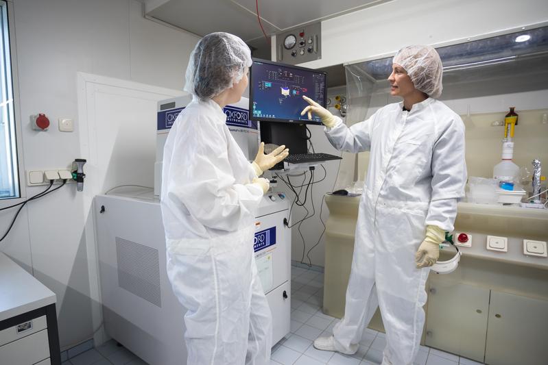
At TU Braunschweig, scientists etch porous semiconductor crystals made of gallium nitride with the utmost precision.
(c) Max Fuhrmann/TU Braunschweig
While computer chips are getting smaller and faster every year, one challenge remains unsolved: combining electronics and photonics on a single chip. Although components such as micro LEDs are available as individual chips and waveguides as tiny fibre optic cables, the materials required are too different for a harmonised chip. A new type of etching process could now be the decisive breakthrough for combining light sources and optical fibres. In the OptoGaN project, researchers from the TU Braunschweig and the Friedrich Schiller University Jena are therefore working on porous gallium nitride.
It will be particularly worthwhile for the strong German photonics industry to take a close look at Braunschweig and Jena over the next few years. The joint idea of the participating research groups offers a wide range of potential applications. The project partners want to realise three of these ideas as demonstrators together with one start-up each. These will then benefit technologies such as waveguides, neuromorphic computers and the Quantum Valley Lower Saxony‘s ion trap quantum computer. At the same time, the newly founded Nitride Technology Centre (NTC) at TU Braunschweig will support the further development of nitride technology at the highest level and bring it into application.
But what are the potential applications for this new technology? For example, quantum computers still need large laser systems to manipulate their ions. If more and more quantum bits are to be calculated together in the computer, this laser system must become significantly smaller – at best the size of a chip. However, the standard material silicon dioxide for waveguides on chips absorbs precisely the critical wavelengths of light. The porous gallium nitride could offer an alternative here and bring the customised light to the individual ion with minimal loss.
Complementary expertise in handling gallium nitride
The porous semiconductor is based on a new selective etching process. The researchers use it to create elongated, air-filled channels – pores – in the gallium nitride structures. This even makes three-dimensional waveguides with complex optical light guidance conceivable. As gallium nitride and the process are compatible with existing LED production methods, integrated electronic and photonic circuits will also be possible.
In order to realise the innovative semiconductor channels for light guidance, the researchers from Braunschweig and Jena are bringing together complementary expertise and special equipment. This is because the etching process used here has both an electronic and a chemical component. Firstly, the Braunschweig researchers produce the base material layer by layer. The semiconductor chip then travels to Jena for ion implantation. The researchers from Jena dope the chip and change its electronic properties in a targeted manner. Finally, the chip has to return to Braunschweig, where the chemical etching process forms the final, porous structure.
About the project
The project Highly integrated microphotonic modules in nitride technologies, OptoGaN for short, is being funded by the Federal Ministry of Education and Research with around 600,000 euros. The TU Braunschweig’s share of the funding amounts to 450,000 euros. The partners from Technische Universität Braunschweig and Friedrich Schiller University Jena started OptoGaN in 2023 for 3 years until October 2026.
Prof. Dr. Andreas Waag
Spokesperson LENA-board
Technische Universität Braunschweig
Institute of Semiconductor Technology
Hans-Sommer-Straße 66
38106 Braunschweig
Phone: +49 531 391-3774
Email: a.waag@tu-braunschweig.de
www.tu-braunschweig.de/iht
www.tu-braunschweig.de/mib/lena
https://qvls.de/en/
https://www.tu-braunschweig.de/en/iht/research/research-projects
https://magazin.tu-braunschweig.de/en/pi-post/integrated-light-as-a-key-to-futur…


A new quantum random number generator is almost 1000 times faster than other generators and much smaller, promising to change data management and cybersecurity in several industries including health, finance, and defense A joint team of researchers led by scientists at King Abdullah University of Science and Technology (KAUST) and King Abdulaziz City for Science and Technology (KACST) has reported the fastest quantum random number generator (QRNG) to date based on international benchmarks. The QRNG, which passed the required randomness…

Very secure and highly efficient: encryption and decryption with luminescent perovskites To guarantee high data security, encryption must be unbreakable while the data remains rapidly and easily readable. A novel strategy for optical encryption/decryption of information has now been introduced in the journal Angewandte Chemie by a Chinese research team. It is based on compounds with carefully modulated luminescent properties that change in response to external stimuli. The compounds are hybrid two-dimensional organic-inorganic metal-halide perovskites, whose structure consists of inorganic…

Researchers at the University of Utah’s Department of Psychiatry and Huntsman Mental Health Institute today published a paper introducing RiskPath, an open source software toolkit that uses Explainable Artificial Intelligence (XAI) to predict whether individuals will develop progressive and chronic diseases years before symptoms appear, potentially transforming how preventive healthcare is delivered. XAI is an artificial intelligence system that can explain complex decisions in ways humans can understand. The new technology represents a significant advancement in disease prediction and prevention…

Researchers train AI to predict if and why proteins form sticky clumps, a mechanism linked to 50 human diseases affecting half a billion people An AI tool has made a step forward in translating the language proteins use to dictate whether they form sticky clumps similar to those linked to Alzheimer’s Disease and around fifty other types of human disease. In a departure from typical “black-box” AI models, the new tool, CANYA, was designed to be able to explain its…


