


Feeding 9 Billion: Innovations in Agricultural Modeling
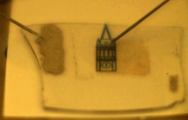
Gif of the device in action. Probes inject positive and negative charges in the light emitting device, which is transparent under the campanile outline, producing bright light.
Credit: Javey lab.
The device opens the door to invisible displays on walls and windows – displays that would be bright when turned on but see-through when turned off — or in futuristic applications such as light-emitting tattoos, according to the researchers.
“The materials are so thin and flexible that the device can be made transparent and can conform to curved surfaces,” said Der-Hsien Lien, a postdoctoral fellow at UC Berkeley and a co-first author along with Matin Amani and Sujay Desai, both doctoral students in the Department of Electrical Engineering and Computer Sciences at Berkeley.
Their study was published March 26 in the journal Nature Communications. The work was funded by the National Science Foundation and the Department of Energy.
The device was developed in the laboratory of Ali Javey, professor of Electrical Engineering and Computer Sciences at Berkeley. In 2015, Javey's lab published research in the journal Science showing that monolayer semiconductors are capable of emitting bright light, but stopped short of building a light-emitting device.
The new work in Nature Communications overcame fundamental barriers in utilizing LED technology on monolayer semiconductors, allowing for such devices to be scaled from sizes smaller than the width of a human hair up to several millimeters. That means that researchers can keep the thickness small, but make the lateral dimensions (width and length) large, so that the light intensity can be high.
Commercial LEDs consist of a semiconductor material that is electrically injected with positive and negative charges, which produce light when they meet. Typically, two contact points are used in a semiconductor-based light emitting device; one for injecting negatively charged particles and one injecting positively charged particles. Making contacts that can efficiently inject these charges is a fundamental challenge for LEDs, and it is particularly challenging for monolayer semiconductors since there is so little material to work with.
The Berkeley research team engineered a way to circumvent this challenge by designing a new device that only requires one contact on the semiconductor. By laying the semiconductor monolayer on an insulator and placing electrodes on the monolayer and underneath the insulator, the researchers could apply an AC signal across the insulator. During the moment when the AC signal switches its polarity from positive to negative (and vice versa), both positive and negative charges are present at the same time in the semiconductor, creating light.
The researchers showed that this mechanism works in four different monolayer materials, all of which emit different colors of light.
This device is a proof-of-concept, and much research still remains, primarily to improve efficiency. Measuring this device's efficiency is not straightforward, but the researchers think it's about 1 percent efficient. Commercial LEDs have efficiencies of around 25 to 30 percent.
The concept may be applicable to other devices and other kinds of materials, the device could one day have applications in a number of fields where having invisible displays are warranted. That could be an atomically thin display that's imprinted on a wall or even on human skin.
“A lot of work remains to be done and a number of challenges need to be overcome to further advance the technology for practical applications,” Javey said. “However, this is one step forward by presenting a device architecture for easy injection of both charges into monolayer semiconductors.”


A new quantum random number generator is almost 1000 times faster than other generators and much smaller, promising to change data management and cybersecurity in several industries including health, finance, and defense A joint team of researchers led by scientists at King Abdullah University of Science and Technology (KAUST) and King Abdulaziz City for Science and Technology (KACST) has reported the fastest quantum random number generator (QRNG) to date based on international benchmarks. The QRNG, which passed the required randomness…

Very secure and highly efficient: encryption and decryption with luminescent perovskites To guarantee high data security, encryption must be unbreakable while the data remains rapidly and easily readable. A novel strategy for optical encryption/decryption of information has now been introduced in the journal Angewandte Chemie by a Chinese research team. It is based on compounds with carefully modulated luminescent properties that change in response to external stimuli. The compounds are hybrid two-dimensional organic-inorganic metal-halide perovskites, whose structure consists of inorganic…

Researchers at the University of Utah’s Department of Psychiatry and Huntsman Mental Health Institute today published a paper introducing RiskPath, an open source software toolkit that uses Explainable Artificial Intelligence (XAI) to predict whether individuals will develop progressive and chronic diseases years before symptoms appear, potentially transforming how preventive healthcare is delivered. XAI is an artificial intelligence system that can explain complex decisions in ways humans can understand. The new technology represents a significant advancement in disease prediction and prevention…

Researchers train AI to predict if and why proteins form sticky clumps, a mechanism linked to 50 human diseases affecting half a billion people An AI tool has made a step forward in translating the language proteins use to dictate whether they form sticky clumps similar to those linked to Alzheimer’s Disease and around fifty other types of human disease. In a departure from typical “black-box” AI models, the new tool, CANYA, was designed to be able to explain its…


