


Feeding 9 Billion: Innovations in Agricultural Modeling
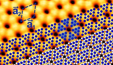
The STM image shows blue phosphorus on a gold substrate. The calculated atomic positions of the slightly elevated P atoms are shown in blue, the lower lying ones in white. Groups of six elevated P atoms appear as triangles.
Credit: HZB
In this form, the phosphorus atoms arrange in a honeycomb structure similar to graphene, however, not completely flat but regularly “buckled”.
Model calculations showed that blue phosphorus is not a narrow gap semiconductor like black phosphorus in the bulk but possesses the properties of a semiconductor with a rather large band gap of 2 electron volts. This large gap, which is seven times larger than in bulk black phosphorus, is important for optoelectronic applications.
Blue P examined at BESSY II
In 2016, blue phosphorus was successfully stabilized on a gold substrate by evaporation. Nevertheless, only now we know for certain that the resulting material is indeed blue phosphorus. To this end, a team from HZB around Evangelos Golias has probed the electronic band structure of the material at BESSY II.
They were able to measure by angle-resolved photoelectron spectroscopy the distribution of electrons in its valence band, setting the lower limit for the band gap of blue phosphorus.
Band structure influenced by the substrate
They found that the P atoms do not arrange independently of the gold substrate but try to adjust to the spacings of the Au atoms. This distorts the corrugated honeycomb lattice in a regular manner which in turn affects the behavior of electrons in blue phosphorus.
As a result, the top of the valence band that defines the one end of the semiconducting band gap agrees with the theoretical predictions about its energy position but is somewhat shifted.
Outlook: optoelectronic applications
“So far, researchers have mainly used bulk black phosphorus to exfoliate atomically thin layers”, Prof. Oliver Rader, head of HZB-Department Materials for green spintronics explains. “These also show a large semiconducting band gap but do not possess the honeycomb structure of blue phosphorus and, above all, cannot be grown directly on a substrate.
Our work not only reveals all the material properties of this novel two-dimensional phosphorus allotrope but highlights the impact of the supporting substrate on the behavior of electrons in blue phosphorus, an essential parameter for any optoelectronic application.”


The NSF-DOE Vera C. Rubin Observatory in Chile has unveiled the very first “mega” images of the cosmos obtained thanks to the extraordinary features and wide-field view of its LSST camera—the largest in the world. The camera took nearly two decades to build and involved hundreds of scientists across the globe, including a number of CNRS teams. The world-wide First Look unveiling event is held on 23 June at the National Academy of Sciences in Washington, D.C. The impressive, car-sized…

Astronomers have created a galactic masterpiece: an ultra-detailed image that reveals previously unseen features in the Sculptor Galaxy. Using the European Southern Observatory’s Very Large Telescope (ESO’s VLT), they observed this nearby galaxy in thousands of colours simultaneously. By capturing vast amounts of data at every single location, they created a galaxy-wide snapshot of the lives of stars within Sculptor. “Galaxies are incredibly complex systems that we are still struggling to understand,” says ESO researcher Enrico Congiu, who led a…

NASA spacecraft make progress in final commissioning, preliminary science operations SAN ANTONIO — June 10, 2025 — Southwest Research Institute’s Dr. Craig DeForest discussed the latest accomplishments of NASA’s PUNCH (Polarimeter to Unify the Corona and Heliosphere) mission during a media event at the 246th American Astronomical Society meeting in Anchorage, Alaska. As the spacecraft constellation completes commissioning, early PUNCH data showed coronal mass ejections, or CMEs, as they erupted from the Sun and traveled across the inner solar system….

Using advanced computational modelling, a research team led by the University of Oxford, working in partnership with the Instituto Superior Técnico in the University of Lisbon, has achieved the first-ever real-time, three-dimensional simulations of how intense laser beams alter the ‘quantum vacuum’—a state once assumed to be empty, but which quantum physics predicts is full of virtual electron-positron pairs. Excitingly, these simulations recreate a bizarre phenomenon predicted by quantum physics, known as vacuum four-wave mixing. This states that the combined…


