


Feeding 9 Billion: Innovations in Agricultural Modeling
Additive printing processes for flexible touchscreens: increased materials and cost efficiency
Free within this context; source: INM
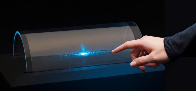
In addition to foldable smartphones, the industry's big players are also working on flexible displays. Until now, touchscreens have been rigid and do not yield to the anatomical shapes of their wearers. They work because they have fine conductive structures near their surfaces.
When the fingers of the user tap on them or wipe them, electronically readable capacities change. For curved surfaces, such conductive tracks are applied to flexible materials such as plastic foils.
Common processes for this are time-consuming or costly because they either involve many process steps or require significant quantities of raw materials or expensive raw materials.
The INM – Leibniz Institute for New Materials has developed new processes with photochemical metallization and printing (gravure printing, inkjet printing) of transparent conductive oxides (TCOs), which are significantly more time- and cost-saving. These will be presented by the scientists at this year's Hannover Messe from 1 to 5 April at Stand C54 in Hall 5.
“Most processes for conductor paths are subtractive: metal is first applied over the entire surface and the excess metal is removed in further process steps. These classic processes, such as sputtering in a high vacuum and subsequent lithography, consume large amounts of silver,” explains Peter W. de Oliveira, head of the InnovationCenter at INM.
“Our processes go the other way round: Conductor tracks are printed or deposited only where they are needed. Expensive high-vacuum technology is not needed for this. This new additive process saves time and money,” de Oliveira summarizes the advantages of the new developments.
In photochemical metallization, colorless silver compounds are converted into electrically conductive silver with the aid of a photoactive layer when exposed to UV light. UV lasers can be used to “write” conductive tracks; UV-transparent photomasks or transparent stamps, which mechanically displace the silver compound, are suitable for larger-scale applications. This makes it possible to down-scale the conductive paths to a width of about one thousandth of a millimeter.
In another innovative process scientists use nanoparticle inks with TCOs such as indium tin oxide (ITO), for inkjet or gravure printing. “We use the TCOs to produce nanoparticles with special properties,” explains de Oliveira. “The TCO ink is then produced by adding a solvent and a special binder. Not only does it ensure that the TCO nanoparticles adhere well to the film, it also increases the flexibility of the TCO coating: this ensures that the conductivity is maintained when the films are bent. This makes it possible to produce highly flexible transparent conductor structures, for example for touch sensors or displays, in a simple printing process”.
The coating is functional after it has been cured at low temperatures below 130 degree Celsius with UV light.
Your expert at INM:
Dr. Peter William de Oliveira
Head Optical Materials
Head InnovationCenter INM
Phone: +49681-9300-148
peter.oliveira@leibniz-inm.de
https://www.youtube.com/watch?v=U7F1XeUOy5g


The majority of Earth’s water is unfit for human consumption since it is trapped in salty oceans. Although desalination plants are capable of turning saltwater into freshwater, they usually use a lot of energy. Scientists have now created a novel, sponge-like substance that effectively turns saltwater into drinkable water when combined with sunlight and a basic plastic cover. Their research, which was published in ACS Energy Letters, shows that an outdoor proof-of-concept that used just natural sunlight to successfully produce…

The scientific team led by Dr. Miloslav Polášek at IOCB Prague has come up with a technique to separate and purify rare earth elements (lanthanides). These are critical to industries ranging from electronics and medicine to automotive and defense. This novel method enables the extraction of metals like neodymium and dysprosium from used neodymium magnets. It is an important component in electric vehicles and wind turbines. Eco-Friendly and Solvent-Free Process Unlike conventional methods that rely on harsh chemicals and generate…

Inserting a nanometer-thin spacer in ExUC-OLEDs improves energy transfer, enhances blue light emission 77-fold, paving way for lightweight, low-voltage, and more flexible OLEDs Organic light-emitting diodes (OLEDs) have transformed display and lighting technology with their vivid colors, deep contrast, and energy efficiency. As demand grows for lighter, thinner, and more energy-saving devices—especially in wearables, foldables, and portable electronics—there’s increasing interest in OLEDs that can operate at lower voltages without compromising performance. A new type of OLEDs, known as exciplex upconversion…

Tokyo, Japan—The COVID-19 pandemic increased public awareness of the importance of mask use for personal protection. However, when the mesh size of mask fabrics is small enough to capture viruses, which are usually around one hundred nanometers in size, the fabric typically also restricts air flow, resulting in user discomfort. But now, researchers from Japan have found a way to avoid this. In a study published this month in Materials Advances, researchers from the Institute of Industrial Science, The University…


