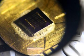
Getting the point: Real-time monitoring of atomic-microscope probes adjusts for wear

Their technique can both dramatically speed up and improve the accuracy of the most precise and delicate nanoscale measurements done with atomic force microscopy (AFM).
If you're trying to measure the contours of a surface with a ruler that's crumbling away as you work, then you at least need to know how fast and to what extent it is being worn away during the measurement.
This has been the challenge for researchers and manufacturers trying to create images of the surfaces of nanomaterials and nanostructures. Taking a photo is impossible at such small scales, so researchers use atomic force microscopes. Think of a device like a phonograph needle being used, on a nanoscale, to measure the peaks and valleys as it's dragged back and forth across a surface. These devices are used extensively in nanoscale imaging to measure the contours of nanostructures, but the AFM tips are so small that they tend to wear down as they traverse the surface being measured.
Today, most researchers stop the measurement to “take a picture” of the tip with an electron microscope, a time-consuming method prone to inaccuracies.
NIST materials engineer Jason Killgore has developed a method for measuring in real time the extent to which AFM tips wear down. Killgore measures the resonant frequency of the AFM sensor tip, a natural vibration rate like that of a tuning fork, while the instrument is in use. Because changes to the size and shape of the tip affect its resonant frequency, he is able to measure the size of the AFM's tip as it works—in increments of a tenth of a nanometer, essentially atomic scale resolution. The technique, called contact resonance force microscopy, is described in a paper recently published in the journal Small.*
The potential impact of this development is considerable. Thousands of AFMs are in use at universities, manufacturing plants and research and development facilities around the world. Improving their ability to measure and image nanosized devices will improve the quality and effectiveness of those devices. Another benefit is that developing new measurement tips—and studying the properties of new materials used in those tips—will be much easier and faster, given the immediate feedback about wear rates.
* J. P. Killgore, R. H. Geiss and D. C. Hurley. Continuous measurement of AFM tip wear by contact resonance force microscopy. Small. Published March 15, 2011.
Media Contact
More Information:
http://www.nist.govAll latest news from the category: Materials Sciences
Materials management deals with the research, development, manufacturing and processing of raw and industrial materials. Key aspects here are biological and medical issues, which play an increasingly important role in this field.
innovations-report offers in-depth articles related to the development and application of materials and the structure and properties of new materials.
Newest articles

Sea slugs inspire highly stretchable biomedical sensor
USC Viterbi School of Engineering researcher Hangbo Zhao presents findings on highly stretchable and customizable microneedles for application in fields including neuroscience, tissue engineering, and wearable bioelectronics. The revolution in…

Twisting and binding matter waves with photons in a cavity
Precisely measuring the energy states of individual atoms has been a historical challenge for physicists due to atomic recoil. When an atom interacts with a photon, the atom “recoils” in…

Nanotubes, nanoparticles, and antibodies detect tiny amounts of fentanyl
New sensor is six orders of magnitude more sensitive than the next best thing. A research team at Pitt led by Alexander Star, a chemistry professor in the Kenneth P. Dietrich…


