Trapping light that doesn't bounce off track for faster electronics

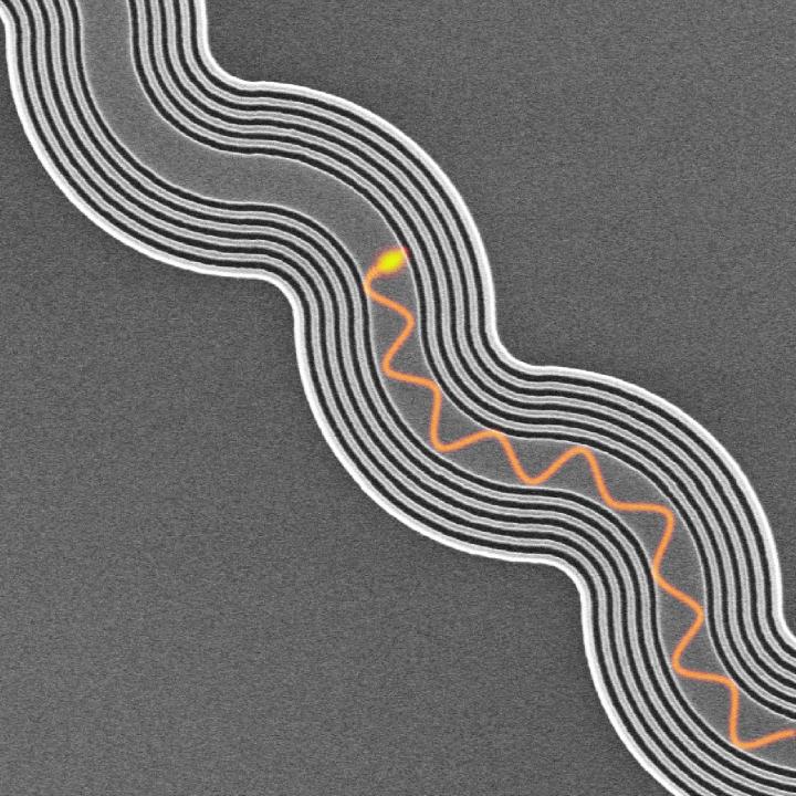
An anisotropic metamaterial waveguide cladding keeps light travel on track throughout a computer chip, preventing leaked and jumbled bits of information.
Credit: Purdue University image/Saman Jahani
A new protective metamaterial “cladding” prevents light from leaking out of the very curvy pathways it would travel in a computer chip.
Because processing information with light can be more efficient than with electrons used in current devices, there is good reason to confine light onto a chip. But light and the bits of information it carries tend to leak and scatter out of the tiny components that must fit on a chip.
A Purdue University-led effort has built a novel cladding along the highways for light travel, called waveguides, to prevent information leaks – particularly around sharp bends where light bounces off track and scatters. Information then gets lost or jumbled rather than communicated throughout a device. Preventing this could facilitate the integration of photonic with electric circuitry, increasing communication speed and reducing power consumption.
“We want the bits of information that we are sending in the waveguide to travel along tight bends and simultaneously not be lost as heat. This is a challenge,” said Zubin Jacob, Purdue assistant professor of electrical and computer engineering.
What makes the waveguide cladding so unique is anisotropy, meaning that the cladding design enables light to travel at different velocities in different directions. By controlling the anisotropy of the cladding, the researchers prevented light from leaking off track into other waveguides where “crosstalk,” or mixing, of information would occur. Instead, bits of information carried by light bounce off by “total internal reflection” and stay strongly confined within a waveguide.
“The waveguide we made is an extreme skin-depth structure, which means that any leakage that does happen will be really small,” said Saman Jahani, Purdue graduate research assistant in electrical and computer engineering. “This approach can pave the way for dense photonic integration on a computer chip without worrying about light leakage.”
###
This work was performed by an international team of researchers at Purdue University, University of Alberta, Texas Tech University, the University of British Columbia and the Shanghai Institute of Microsystem and Information Technology. The team's findings appear in the journal Nature Communications.
Various sources of funding supported the research, including the National Science Foundation, the Chinese Academy of Sciences, the Shanghai Municipal Government, the Natural Sciences and Engineering Research Council of Canada and the Silicon Electronic-Photonic Integrated Circuits Program.
ABSTRACT
Controlling evanescent waves using silicon photonic all-dielectric metamaterials for dense integration
Saman Jahani1,2, Sangsik Kim2,3, Jonathan Atkinson1, Justin C. Wirth2, Farid Kalhor1,2, Abdullah Al Noman2, Ward D. Newman1,2, Prashant Shekhar1, Kyunghun Han2, Vien Van1, Raymond G. DeCorby1, Lukas Chrostowski4, Minghao Qi2,5& Zubin Jacob1,2
1University of Alberta, Demonton, Canada
2Purdue University, West Lafayette, IN, USA
3Texas Tech University, Lubbock, TX, USA
4University of British Columbia, Vancouver, Canada
5Chinese Academy of Sciences, Shanghai, China
doi:10.1038/s41467-018-04276-8
Ultra-compact, densely integrated optical components manufactured on a CMOS-foundry platform are highly desirable for optical information processing and electronic-photonic co-integration. However, the large spatial extent of evanescent waves arising from nanoscale confinement, ubiquitous in silicon photonic devices, causes significant cross-talk and scattering loss. Here, we demonstrate that anisotropic all-dielectric metamaterials open a new degree of freedom in total internal reflection to shorten the decay length of evanescent waves. We experimentally show the reduction of cross-talk by greater than 30 times and the bending loss by greater than 3 times in densely integrated, ultra-compact photonic circuit blocks. Our prototype all-dielectric metamaterial-waveguide achieves a low propagation loss of approximately 3.7±1.0 dB/cm, comparable to those of silicon strip waveguides. Our approach marks a departure from interference-based confinement as in photonic crystals or slot waveguides, which utilize nanoscale field enhancement. Its ability to suppress evanescent waves without substantially increasing the propagation loss shall pave the way for all-dielectric metamaterial-based dense integration.


