Optical packages for encapsulating components at wafer level
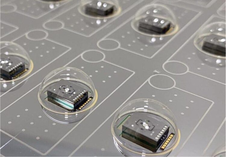
Substrate wafer equipped with scanner mirrors, the encapsulation of the components is realized here with a glass lid wafer.
© Fraunhofer ISIT
New technology kit enables extended functionalities.
Fraunhofer ISIT operates state-of-the-art production lines for processing silicon with a processing accuracy in the nanometer range. These precise structure generation processes have now been successfully transferred to other materials. The shaping of various types of glass has proven to be particularly significant. After all, with the integration of optical functions into the world of microsystems, the packaging of components and systems at wafer level (WLP) is facing new challenges. Future applications, such as augmented and virtual reality in lightweight glasses, require the development of small optical packages.
The process developed at Fraunhofer ISIT allows the fabrication of precise optical components on wafer level for different applications at low cost. This technology has been significantly further developed in recent years. In the meantime, ISIT offers its customers a multifaceted technology platform as a construction kit, which opens up numerous new functionalities.
Since glass has a similar coefficient of thermal expansion (e.g. borosilicate glass) to silicon, it is ideally suited for anodic bonding. This produces a material compound that remains stable even under large temperature changes.
If the silicon wafer is previously provided with structured recesses, the glass can be molded into these embossed structures when the silicon-glass bond is raised to temperatures above the transformation temperature of the glass. The glass then becomes a viscous (highly viscous) fluid that can be pressed into molds, for example, when the external pressure exceeds the gas pressure in the recessed molds. The resulting glass structures are exposed by dissolving the original silicon wafer in a caustic bath.
This process of high viscosity molding has since been further developed at ISIT by using a low gas pressure in suitable furnaces to also form shapes in a glass wafer by blowing. Depending on the temperature budget, glass shapes are formed which are determined only by the viscosity, surface tension and pressure conditions inside and outside the previously created volumes in the silicon wafer.
The surfaces of glass shapes generated in this way are created without material contact and are therefore flat, with roughnesses of less than one nanometer, a must for optical applications. In this way, optical components such as lenses, concave mirrors or domes of high optical quality have been produced from glass at Fraunhofer ISIT. Since these shapes are produced on wafers, a large number of optically identical components are always produced simultaneously, leading to low production costs. The glass packages have already been used as housings for camera chips, light sensors and optical scanners with micromirrors.
In addition to the technological further development of the glass manufacturing processes, simulation programs are now also used at ISIT in order to be able to further optimize the shaping. Optical measurement techniques have been set up to characterize the finished components.
But that is not all. The technology kit also makes it possible to feed electrical contacts through a glass wafer, or to precisely mount individual components such as laser diodes or lens elements on a carrier wafer using high-precision laser soldering, and then to encapsulate them together with a suitable glass wafer. Virtually any desired optical or opto-mechanical assembly can be implemented, operated under vacuum or even filled with various gases.
At Laser 2022, Fraunhofer ISIT will demonstrate the possibilities of the technology building block by building a miniaturized silicon substrate-based RGB laser source and by hermetically capping MEMS micro mirrors for LIDAR systems or projection applications.
Fraunhofer ISIT at LASER World of PHOTONICS 2022: Hall B4, Booth 239.
Wissenschaftliche Ansprechpartner:
Dr. Wolfgang Reinert
Chief of science and technology
wolfgang.reinert@isit.fraunhofer.de
Media Contact
All latest news from the category: Process Engineering
This special field revolves around processes for modifying material properties (milling, cooling), composition (filtration, distillation) and type (oxidation, hydration).
Valuable information is available on a broad range of technologies including material separation, laser processes, measuring techniques and robot engineering in addition to testing methods and coating and materials analysis processes.


Newest articles

Properties of new materials for microchips
… can now be measured well. Reseachers of Delft University of Technology demonstrated measuring performance properties of ultrathin silicon membranes. Making ever smaller and more powerful chips requires new ultrathin…

Floating solar’s potential
… to support sustainable development by addressing climate, water, and energy goals holistically. A new study published this week in Nature Energy raises the potential for floating solar photovoltaics (FPV)…

Skyrmions move at record speeds
… a step towards the computing of the future. An international research team led by scientists from the CNRS1 has discovered that the magnetic nanobubbles2 known as skyrmions can be…

