Laser-based silicon crystallization for monolithic integration in MEMS sensors
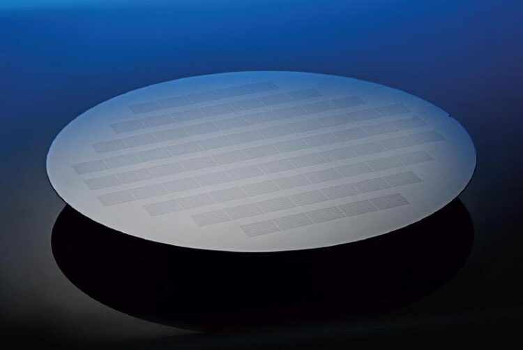
Gentle high-temperature crystallization: Fraunhofer ILT, together with Fraunhofer ISIT and IST, has developed a selective, laser-based crystallization process for the manufacture of MEMS sensor units directly on active circuits.
© Fraunhofer ILT, Aachen, Germany
Micro-electromechanical systems (MEMS) have proven themselves a billion times over as sensors in smart cars, cell phones and mini insulin pumps, among other things.
To make these MEMS even more powerful in the future, researchers at the Fraunhofer Institute for Laser Technology ILT in Aachen have developed a CMOS-compatible deposition and laser crystallization process in collaboration with the Fraunhofer ISIT and IST. In contrast to other common processes, this new process eliminates the need for wires and solder joints, an advantage that can significantly reduce the component size and enhance the sensor performance.
We owe safe and reliable car journeys to MEMS sensors since they record many key parameters of vehicle operation. They make it possible to control many vehicle systems such as airbags, anti-lock brakes or electronic stability programs. To measure acceleration, etc., MEMS inertial sensors are also incorporated into consumer products such as smartphones, smartwatches, quadrocopters, etc. by the billions. So that MEMS sensor units can perform these tasks reliably and safely, they are combined with an electronic, application-specific integrated circuit (ASIC) that sits on a silicon carrier unit (wafer).
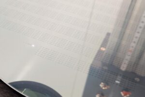
© Fraunhofer ILT, Aachen, Germany
However, because the ambient temperature near the integrated circuit with its temperature-sensitive CMOS transistors may not exceed 450°C, MEMS sensors made of crystalline silicon are first manufactured separately due to the conventionally high manufacturing temperatures. Then they are contacted with the circuit via wire and solder connections or wafer bonding processes. “But conventional interconnection technology requires a relatively large amount of space and prevents further miniaturization of the MEMS,” explains Florian Fuchs, a research associate in the Thin Film Processing group at Fraunhofer ILT. For this reason, MEMS made of crystalline silicon cannot be built directly on the ASIC. The temperature incompatibilities in the manufacturing process make it difficult to further miniaturize the sensors and enhance their performance.
Gentle crystallization of sensitive silicon layers
Instead of using conventional joining techniques, Fraunhofer ILT is relying on a laser-based process which enables it to build MEMS sensors of crystalline silicon directly (monolithically) on the temperature-sensitive circuits. The project focuses on the deposition of Si layers by Fraunhofer IST and ISIT, selective laser crystallization by Fraunhofer ILT, and the design and microelectronic processing of the layers into sensors by Fraunhofer ISIT. The researchers are taking advantage of the fact that amorphous silicon layers can already be produced on the wafer holding the circuit at temperatures below 450°C and high deposition rates. The laser not only crystallizes this silicon layer, but also activates the dopants it contains, thus ensuring suitable electrical conductivity. Subsequently, the sensor units are processed further using classic microelectronic manufacturing processes.
Efficient heat dissipation in three spatial directions
When laser radiation is used to crystallize silicon at high-temperature, but below its melting point, crystallization occurs spatially, selectively and very quickly (in the lower millisecond range). This way – in conjunction with targeted temperature management – the process minimizes mechanical stresses in the layer material, but does not damage the sensitive electronics on the underlying substrate. The silicon is crystallized with a focused laser beam that has a diameter of a few 10 µm and guided by a mirror to scan the entire surface step by step. In this spatially selective process, heat is removed effectively in three spatial directions. This distinguishes the process from alternative photonic processes such as flash exposure (flash lamp), where heat can only be dissipated in one direction because the area to be processed is so large.
“Since the energy is quickly introduced into only a small volume, we achieve solid phase crystallization of the silicon with laser processing at temperatures that are actually above the destruction threshold of the underlying circuit. Due to the short local processing time, the circuit is nevertheless not damaged,” explains Dr. Christian Vedder, head of the Thin Film Processing group at Fraunhofer ILT. The newly developed laser process reduces the electrical resistances of the silicon layers by more than four orders of magnitude, down to below a value of 0.05 Ω*cm. At a layer thickness of 10 µm, this value corresponds to a sheet resistance of 50 Ω/sq. MEMS sensors with typical finger structures for a capacitive acceleration sensor could be produced from these layers.
Advantages for monolithic MEMS integration
“As crystalline silicon layers can be produced under CMOS-compatible conditions on an ASIC wafer, we are opening up new possibilities for integrating MEMS-IC because it is no longer necessary to modify the CMOS manufacturing processes,” says Fraunhofer ILT scientist Fuchs. Since the process constraints have been eliminated, MEMS and IC can be developed independently, thus potentially reducing development time and costs significantly. In addition to increasing integration density, the process eliminates wire connections and bond pads, thus leading to expected lower parasitic interference variables and improved shielding against electromagnetic interference fields. This elimination, in turn, has a positive effect on the signal quality and drift behavior of the sensors.
Interesting applications for the automotive industry, medical technology and fire departments
The knowledge gained here can be broadened and developed in several directions. It would be interesting, for example, to adapt the process to the specific requirements of different sensor types with different layer thicknesses or other doping materials. Fuchs elaborates: “We are now looking for users from industry who can profitably use the process our team has developed for their products.”
The prospect of increased performance combined with miniaturization also makes MEMS technology attractive for other fields of application whose requirements cannot yet be met by today’s MEMS systems. One conceivable application would be in the field of autonomous driving, where very precise acceleration sensors could bridge the gaps in GPS signal reception in tunnels or parking garages. The process also offers interesting potential in medical technology, for example, to integrate temperature sensors into headphones and use the data obtained to monitor patients or to fight pandemics. In addition, miniaturized, high-precision acceleration MEMS sensors could help precisely locate firefighters in burning buildings and thus increase the safety of emergency personnel.
Fraunhofer ILT at electronica
Come and talk to our experts at electronica, the world’s leading trade fair and conference for electronics from November 15 to 18, 2022 in Munich: joint Fraunhofer booth 258 in hall B4.
MUSIC project
The internal project on market-oriented preliminary research, funded by the Fraunhofer-Gesellschaft, involved these institutes:
• Fraunhofer Institute for Laser Technology ILT, Aachen
• Fraunhofer Institute for Silicon Technology ISIT, Itzehoe (project management)
• Fraunhofer Institute for Surface Engineering and Thin Films IST, Braunschweig
Wissenschaftliche Ansprechpartner:
Florian Fuchs M. Sc.
Thin Film Processing Group
Telephone +49 241 8906-676
florian.fuchs@ilt.fraunhofer.de
Dr.- Ing. Christian Vedder
Group Leader Thin Film Processing
Telephone +49 241 8906-378
christian.vedder@ilt.fraunhofer.de
Fraunhofer Institute for Laser Technology ILT
Steinbachstraße 15
52074 Aachen, Germany
Weitere Informationen:
https://www.ilt.fraunhofer.de/en.html
https://electronica.de/en/
Media Contact
All latest news from the category: Process Engineering
This special field revolves around processes for modifying material properties (milling, cooling), composition (filtration, distillation) and type (oxidation, hydration).
Valuable information is available on a broad range of technologies including material separation, laser processes, measuring techniques and robot engineering in addition to testing methods and coating and materials analysis processes.


Newest articles

Silicon Carbide Innovation Alliance to drive industrial-scale semiconductor work
Known for its ability to withstand extreme environments and high voltages, silicon carbide (SiC) is a semiconducting material made up of silicon and carbon atoms arranged into crystals that is…

New SPECT/CT technique shows impressive biomarker identification
…offers increased access for prostate cancer patients. A novel SPECT/CT acquisition method can accurately detect radiopharmaceutical biodistribution in a convenient manner for prostate cancer patients, opening the door for more…

How 3D printers can give robots a soft touch
Soft skin coverings and touch sensors have emerged as a promising feature for robots that are both safer and more intuitive for human interaction, but they are expensive and difficult…

