The Transistor out of the Printer
Electronic components can be printed on flexible substrates such as paper or polymer. This requires specialized printing equipment.
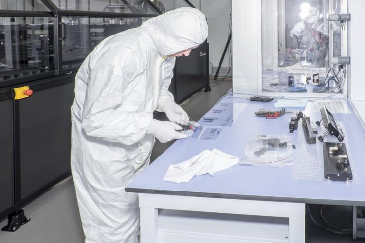
Image: Empa
A new revolution in the production of electronic circuits is on the way: Empa researchers are working on electronics that come out of printers. This makes it possible to produce the circuits on all sorts of substrates, such as paper or plastic film – but there are still some hurdles to overcome.
Imagine being able to easily print electronics on any surface. Today, this is no longer a utopia: “Printed Electronics” is an emerging techno logy that makes it possible to apply circuits to various substrates – using ink and special printers. This is by no means a small market: A new report by the industry association for organic and printed electronics shows that the sector has already developed into a global market worth more than 35 billion US dollars – a market that is expected to continue growing strongly in the coming years.
Traditionally, the manufacturing of electronics has been a complex process that requires expensive equipment. However, the Internet of Things requires a new type of electronics: The circuits no longer have to be as tiny and fast as possible at all costs, but cheap and easy to manufacture – and at the same time they should be realizable on thin and flexible substrates. This includes RFIDs on product packaging, for example. In the future, applications are also conceivable for simple sensors on milk cartons, which indicate when the contents are no longer consumable, or on frozen products, which signal whether the cold chain has been interrupted.
Transistors on Paper and Film
Empa researchers Jakob Heier from the Laboratory for Functional Polymers and Yaroslav Romanyuk from the Laboratory for Thin Films and Photovoltaics are working with their teams to advance the technology. Together with researchers from the Paul Scherrer Institute and EPFL Lausanne, they are working on the “FOXIP” research project, short for “Functional OXIdes Printed on Polymers and Paper”. The aim of the project is to print thin-film transistors on paper and PET films – using a printing technique that could be suitable for use in industry. Inks in which tiny particles of metal oxides are dissolved are used for this. These are applied to the substrate using various printing techniques – contact printing or an inkjet printer. “Of course, we don’t use ordinary office printers for this, but highly specialized equipment,” explains Romanyuk. At Empa’s Coating Competence Center these printing devices can be found.
But to be able to reliably print circuits on flexible substrates, a number of challenges must first be solved: From the optimization of the substrate itself, to the composition of the ink and the accuracy of the printing technology, to the thermal curing of the layers without damaging the paper or film.
Starting with the printing substrate: Often this is flexible – for example, paper or a polymer film – and does not have a completely smooth surf-ace, as is the case with silicon wafers, which are used for the manufacture of conventional electronic components. This makes it much more difficult to achieve the necessary precision in the manufacture of the circuits. As a result, the components of printed electronics are currently about a factor of 1,000 larger than microelectronics produced by the conventional manufacturing process. “But that doesn’t mean that the circuits are huge: We’re talking about printing with accuracies in the range of ten micrometers, which is less than the diameter of a hair,” Heier explains.
Materials in ink form
Another major challenge is how conductive, semi-conductive and insulating materials, which are necessary for the construction of circuits, can be brought into ink form – and how they can be turned into a continuous material with the desired properties after the printing process.
Jakob Heier is researching how these special inks are constructed. An ink includes two parts: small particles of the functional material and solvents that evaporate on their own after application. However, these two components are often not sufficient: Additional binders and additives must be added to make the ink stable and printable. But these are a problem: if they remain in the layer after application, they disturb the desired function of the circuits. They must therefore be burnt out. However, this requires relatively high temperatures – and this in turn can damage the paper or film on which the electronics are printed.
Heier and his team are working on developing a printable ink for graphene layers that only requires the graphene particles and the solvent – in other words, no additives that have to be burnt out. The printed layers should be stable enough to retain the same conductive properties – regardless of whether the substrate material including the printed layer is bent or even twisted. “If this is successful, we will be a big step closer to printing on polymer or paper: at least the printing of conductive tracks will then no longer require post-treatment at elevated temperatures,” Heier explains
With Flashes from the Ink to the Transistor
The situation is different with inks based on metal oxide nanoparticles. Here, the so-called sintering, i.e. the thermal treatment of the printed layers, is necessary in order to recombine the individual particles dissolved in the ink and thus obtain a functional layer. However, both paper and the films used are very sensitive to temperature. Ideally, therefore, only the metal oxide layers should be heated – but the substrate should remain cool. “We use a method called ’flash sintering’,” explains Romanyuk. The printed layer is heated with ultra-short flashes, so fast that the substrate material is not heated.
Materials based on metal oxides are a promising material class for printed electronics: they can be conductive, semiconductive or insulating. Compared to inks based on organic materials, oxide materials have a higher electron mobility, which means they have the potential to increase the performance of printed electronic circuit elements. At the same time, the oxide materials are more stable when exposed to air. “Especially exciting is indium tin oxide: It is both highly conductive and transparent at the same time,” Romanyuk explains. His team recently succeeded in printing oxide-based field-effect transistors using an inkjet printer, which could make it possible to create transparent circuits on a transparent substrate in the future. Thanks to the possibilities offered by the Coating Competence Center (CCC) at Empa, the results of the two research groups are not limited to the laboratory. “The printing technologies developed are based on equipment with which industry is already working,” explains Romanyuk. This enables a rapid transition from scientific breakthroughs to the industrial production of new printed electronics.
Wissenschaftliche Ansprechpartner:
Dr. Yaroslav Romanyuk
Thin Films and Photovoltaics
Phone +41 58 765 41 69
Yaroslav.Romanyuk@empa.ch
Dr. Jakob Heier
Functional Polymers
Phone +41 58 765 4356
jakob.heier@empa.ch
Weitere Informationen:
Media Contact
All latest news from the category: Power and Electrical Engineering
This topic covers issues related to energy generation, conversion, transportation and consumption and how the industry is addressing the challenge of energy efficiency in general.
innovations-report provides in-depth and informative reports and articles on subjects ranging from wind energy, fuel cell technology, solar energy, geothermal energy, petroleum, gas, nuclear engineering, alternative energy and energy efficiency to fusion, hydrogen and superconductor technologies.


Newest articles

Superradiant atoms could push the boundaries of how precisely time can be measured
Superradiant atoms can help us measure time more precisely than ever. In a new study, researchers from the University of Copenhagen present a new method for measuring the time interval,…

Ion thermoelectric conversion devices for near room temperature
The electrode sheet of the thermoelectric device consists of ionic hydrogel, which is sandwiched between the electrodes to form, and the Prussian blue on the electrode undergoes a redox reaction…

Zap Energy achieves 37-million-degree temperatures in a compact device
New publication reports record electron temperatures for a small-scale, sheared-flow-stabilized Z-pinch fusion device. In the nine decades since humans first produced fusion reactions, only a few fusion technologies have demonstrated…

