New technique lets researchers map strain in next-gen solar cells
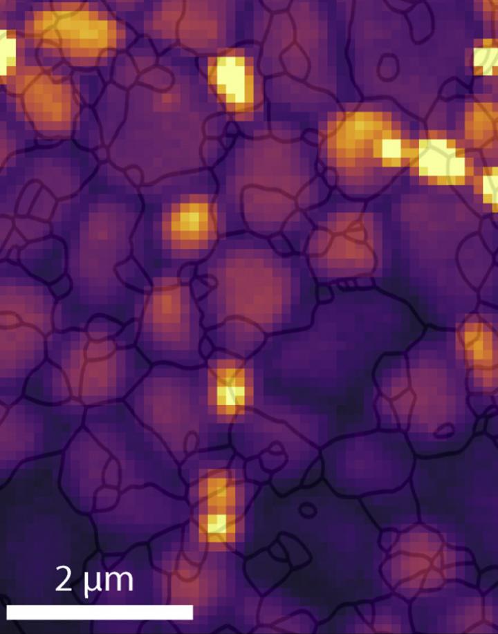
The thin lines show the grain structure of a perovskite solar cell obtained using a new type of electron backscatter diffraction. Researchers can use a different technique to map sites of high energy loss (dark purple) and low energy loss (yellow). Credit: Jariwala et al., Joule, 2019
In order to understand where strain builds up within a solar cell and triggers the energy loss, scientists must visualize the underlying grain structure of perovskite crystals within the solar cell. But the best approach involves bombarding the solar cell with high-energy electrons, which essentially burns the solar cell and renders it useless.
Researchers from the University of Washington and the FOM Institute for Atomic and Molecular Physics in the Netherlands have developed a way to illuminate strain in lead halide perovskite solar cells without harming them.
Their approach, published online Sept. 10 in Joule, succeeded in imaging the grain structure of a perovskite solar cell, showing that misorientation between microscopic perovskite crystals is the primary contributor to the buildup of strain within the solar cell.
Crystal misorientation creates small-scale defects in the grain structure, which interrupt the transport of electrons within the solar cell and lead to heat loss through a process known as non-radiative recombination.
“By combining our optical imaging with the new electron detector developed at FOM, we can actually see how the individual crystals are oriented and put together within a perovskite solar cell,” said senior author David Ginger, a UW professor of chemistry and chief scientist at the UW-based Clean Energy Institute.
“We can show that strain builds up due to the grain orientation, which is information researchers can use to improve perovskite synthesis and manufacturing processes to realize better solar cells with minimal strain — and therefore minimal heat loss due to non-radiative recombination.”
Lead halide perovskites are cheap, printable crystalline compounds that show promise as low-cost, adaptable and efficient alternatives to the silicon or gallium arsenide solar cells that are widely used today. But even the best perovskite solar cells lose some electricity as heat at microscopic locations scattered across the cell, which dampens the efficiency.
Scientists have long used fluorescence microscopy to identify the locations on perovskite solar cells' surface that reduce efficiency. But to identify the locations of defects causing the heat loss, researchers need to image the true grain structure of the film, according to first author Sarthak Jariwala, a UW doctoral student in materials science and engineering and a Clean Energy Institute Graduate Fellow.
“Historically, imaging the solar cell's underlying true grain structure has not been possible to do without damaging the solar cell,” said Jariwala.
Typical approaches to view the internal structure utilize a form of electron microscopy called electron backscatter diffraction, which would normally burn the solar cell. But scientists at the FOM Institute for Atomic and Molecular Physics, led by co-authors Erik Garnett and Bruno Ehrler, developed an improved detector that can capture electron backscatter diffraction images at lower exposure times, preserving the solar cell structure.
The images of perovskite solar cells from Ginger's lab reveal a grain structure that resembles a dry lakebed, with “cracks” representing the boundaries among thousands of individual perovskite grains. Using this imaging data, the researchers could for the first time map the 3D orientation of crystals within a functioning perovskite solar cell. They could also determine where misalignment among crystals created strain.
When the researchers overlaid images of the perovskite's grain structure with centers of non-radiative recombination, which Jariwala imaged using fluorescence microscopy, they discovered that non-radiative recombination could also occur away from visible boundaries.
“We think that strain locally deforms the perovskite structure and causes defects,” said Ginger. “These defects can then disrupt the transport of electrical current within the solar cell, causing non-radiative recombination — even elsewhere on the surface.”
While Ginger's team has previously developed methods to “heal” some of these defects that serve as centers of non-radiative recombination in perovskite solar cells, ideally researchers would like to develop perovskite synthesis methods that would reduce or eliminate non-radiative recombination altogether.
“Now we can explore strategies like controlling grain size and orientation spread during the perovskite synthesis process,” said Ginger. “Those might be routes to reduce misorientation and strain — and prevent defects from forming in the first place.”
###
Co-authors on the paper are Hongyu Sun, Gede Adhyaksa, Adries Lof and Loreta Muscarella with the FOM Institute for Atomic and Molecular Physics. The research was funded by the U.S. Department of Energy, U.S. National Science Foundation, the UW Clean Energy Institute, TKI Urban Energy, the European Research Council and the Dutch Science Foundation.
For more information, contact Ginger at 206-685-2231 or dginger@uw.edu.
Grant numbers: DE-SC0013957, DGE-1633216, TEID215022, 337328
Link to full release: https:/
James Urton
University of Washington
206-543-2580
jurton@uw.edu
Media Contact
All latest news from the category: Power and Electrical Engineering
This topic covers issues related to energy generation, conversion, transportation and consumption and how the industry is addressing the challenge of energy efficiency in general.
innovations-report provides in-depth and informative reports and articles on subjects ranging from wind energy, fuel cell technology, solar energy, geothermal energy, petroleum, gas, nuclear engineering, alternative energy and energy efficiency to fusion, hydrogen and superconductor technologies.


Newest articles

Superradiant atoms could push the boundaries of how precisely time can be measured
Superradiant atoms can help us measure time more precisely than ever. In a new study, researchers from the University of Copenhagen present a new method for measuring the time interval,…

Ion thermoelectric conversion devices for near room temperature
The electrode sheet of the thermoelectric device consists of ionic hydrogel, which is sandwiched between the electrodes to form, and the Prussian blue on the electrode undergoes a redox reaction…

Zap Energy achieves 37-million-degree temperatures in a compact device
New publication reports record electron temperatures for a small-scale, sheared-flow-stabilized Z-pinch fusion device. In the nine decades since humans first produced fusion reactions, only a few fusion technologies have demonstrated…

