Lead Halide Perovskites – a Horse of a Different Color
Horse Graphic
Y. Vaynzof
In a joint experimental and theoretical effort between Lund University (Sweden), the Russian Academy of Science (Russia), and the Center for Advancing Electronics Dresden at Technische Universität Dresden (Germany), researchers developed a novel spectroscopic technique for the study of charge carrier dynamics in lead halide perovskites – publication in the renowned journal Nature Communications.
Metal halide perovskites have been under intense investigation over the last decade due to the remarkable rise in their performance in optoelectronic devices such as solar cells or light-emitting diodes. Despite tremendous progress in this field, many fundamental aspects of the photophysics of perovskite materials remain unknown, such as a detailed understanding of their defect physics and charge recombination mechanisms.
These are typically studied by measuring the photoluminescence – i.e. the emission of light upon photoexcitation – of the material in both the steady-state and transient regimes. While such measurements are ubiquitous in literature, they do not capture the full range of the photophysical processes that occur in metal halide perovskites and thus represent only a partial picture of their charge carrier dynamics. Moreover, while several theories are commonly applied to interpret these results, their validity and limitations have not been explored, raising concerns regarding the insights they offer.
I. Scheblykin / Y. Vaynzof
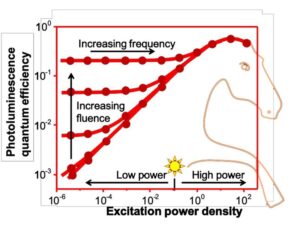
To tackle this challenging question, a trinational team of researchers from Lund University (Sweden), the Russian Academy of Science (Russia) and the Technical University of Dresden (Germany) have developed a new methodology for the study of lead halide perovskites. This methodology is based on the complete mapping of the photoluminescence quantum yield and decay dynamics in the two-dimensional (2D) space of both fluence and frequency of the excitation light pulse. Such 2D maps not only offer a complete representation of the sample’s photophysics, but also allow to examine the validity of theories, by applying a single set of theoretical equations and parameters to the entire data set.
“Mapping a perovskite film using our new method is like taking its fingerprints – it provides us with a great deal of information about each individual sample.” says Prof. Ivan Scheblykin, a Professor of Chemical Physics at Lund University. “Interestingly, each map resembles the shape of a horse’s neck and mane, leading us to fondly refer to them as ‘perovskite horses’, which are all unique in their own way.”
“The wealth of information contained in each 2D map allows us to explore different possible theories that may explain the complex behavior of charge carriers in metal halide perovskites” adds Dr. Pavel Frantsuzov from the Siberian Brunch of the Russian Academy of Science. Indeed, the researchers discovered that the two most commonly applied theories (the so called ‘ABC theory’ and the Shockley-Read-Hall theory) cannot explain the 2D maps across the entire range of excitation parameters. They propose a more advanced theory that includes additional nonlinear processes to explain the photophysics of metal halide perovskites.
The researchers show that their method has important implications for the development of more efficient perovskite solar cells. Prof. Dr. Yana Vaynzof, Chair for Emerging Electronic Technologies at the Institute for Applied Physics and Photonic Materials and the Center for Advancing Electronics Dresden (cfaed) explains: “By applying the new methodology to perovskite samples with modified interfaces, we were able to quantify their influence on the charge carrier dynamics in the perovskite layer by changing, for example, the density and efficacy of traps. This will allow us to develop interfacial modification procedures that will lead to optimal properties and more efficient photovoltaic devices.”
Importantly, the new method is not limited to the study of metal halide perovskites and can be applied to any semiconducting material. “The versatility of our method and the ease with which we can apply it to new material systems is very exciting! We anticipate many new discoveries of fascinating photophysics in novel semiconductors.” adds Prof. Scheblykin.
The work was now published in the prestigious journal “Nature Communications”.
About cfaed
cfaed is a research cluster at TU Dresden (TUD). As an interdisciplinary research center for perspectives of electronics, it is located at the TUD as a central scientific unit, but also integrates nine non-university research institutions in Saxony as well as TU Chemnitz as cooperating institutes. With its vision, the cluster aims to shape the future of electronics and initiate revolutionary new applications, such as electronics that do not require boot time, are capable of THz imaging, or support complex biosensor technology. These innovations make conceivable performance improvements and applications that would not be possible with the continuation of today’s silicon chip-based technology. In order to achieve its goals, cfaed combines the thirst for knowledge of the natural sciences with the innovative power of engineering.
www.cfaed.tu-dresden.de
Wissenschaftliche Ansprechpartner:
Prof. Ivan G. Scheblykin
Professor of Chemical Physics, Department of Chemistry, Lund University, Sweden
Tel. +46 46 222 48 48
E-Mail: ivan.scheblykin@chemphys.lu.se
Dr. Pavel Frantsuzov
Head of Theoretical Chemistry Lab
Voevodsky Institute of Chemical Kinetics and Combustion
Siberian Brunch of the Russian Academy of Science
Tel. +7 383 333-2855
E-Mail: pavel.frantsuzov@gmail.com
Prof. Dr. Yana Vaynzof
Chair for Emerging Electronic Technologies at the Institute for Applied Physics and Center for Advancing Electronics Dresden – cfaed at TU Dresden
Tel. +49 351 463-42132
E-Mail: yana.vaynzof@tu-dresden.de
Originalpublikation:
Title: Are Shockley-Read-Hall and ABC models valid for lead halide perovskites?
Authors: Alexander Kiligaridis, Pavel Frantsuzov, Aymen Yangui, Sudipta Seth, Jun Li, Qingzhi An, Yana Vaynzof and Ivan G. Scheblykin
Nature Communications 12, Article number: 3329 (2021)
DOI: 10.1038/s41467-021-23275-w
Link: https://www.nature.com/articles/s41467-021-23275-w
Media Contact
All latest news from the category: Power and Electrical Engineering
This topic covers issues related to energy generation, conversion, transportation and consumption and how the industry is addressing the challenge of energy efficiency in general.
innovations-report provides in-depth and informative reports and articles on subjects ranging from wind energy, fuel cell technology, solar energy, geothermal energy, petroleum, gas, nuclear engineering, alternative energy and energy efficiency to fusion, hydrogen and superconductor technologies.


Newest articles

Silicon Carbide Innovation Alliance to drive industrial-scale semiconductor work
Known for its ability to withstand extreme environments and high voltages, silicon carbide (SiC) is a semiconducting material made up of silicon and carbon atoms arranged into crystals that is…

New SPECT/CT technique shows impressive biomarker identification
…offers increased access for prostate cancer patients. A novel SPECT/CT acquisition method can accurately detect radiopharmaceutical biodistribution in a convenient manner for prostate cancer patients, opening the door for more…

How 3D printers can give robots a soft touch
Soft skin coverings and touch sensors have emerged as a promising feature for robots that are both safer and more intuitive for human interaction, but they are expensive and difficult…

