Enhancing solar efficiency with upconversion
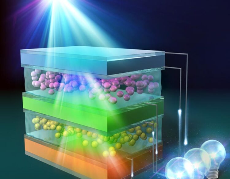
Semiconductor bonding mediated by upconversion material
Credit: KyotoU/Katsuaki Tanabe
Wafer bonding technology improves photovoltaics.
Solar cell technologies have been improving incrementally over the decades, but energy conversion has remained less than optimal.
Now, researchers at Kyoto University have developed a novel wafer bonding technology using an optical upconversion material that transforms sunlight to shorter-wavelengths. This new semiconductor process utilizes the interface’s optical function for bond formation.
The team created a stacked structure consisting of a thin silicon film mimicking the upper subcell of a multi-junction solar cell and a silicon solar cell wafer; these layers were bonded with an adhesive made from upconversion nanoparticles dispersed in a hydrogel.
Conventional multi-junction solar cells are created with the vapor phase growth method. However, this method is limited by lattice matching in semiconductor materials.
The team, led by Katsuaki Tanabe, have applied their wafer bonding method to the production of a range of optical and electronic devices, demonstrating that different semiconductor materials can be stacked in any combination without the restriction of lattice matching.
“Even inherently non-absorbed light of longer wavelengths in the lower subcell of a multi-junction solar cell could be used to enhance the efficiency of the overall energy conversion via our upconverting interface,” concludes the author.
The paper “Upconversion semiconductor interfaces by wafer bonding for photovoltaic applications” appeared on 6 July 2022 in Applied Physics Letters, with doi: 10.1063/5.0097427
About Kyoto University
Kyoto University is one of Japan and Asia’s premier research institutions, founded in 1897 and responsible for producing numerous Nobel laureates and winners of other prestigious international prizes. A broad curriculum across the arts and sciences at both undergraduate and graduate levels is complemented by numerous research centers, as well as facilities and offices around Japan and the world.
For more information please see: http://www.kyoto-u.ac.jp/en
Media Contact
Jake G. Tobiyama
Kyoto University
tobiyama.gakuji.6y@kyoto-u.ac.jp
All latest news from the category: Power and Electrical Engineering
This topic covers issues related to energy generation, conversion, transportation and consumption and how the industry is addressing the challenge of energy efficiency in general.
innovations-report provides in-depth and informative reports and articles on subjects ranging from wind energy, fuel cell technology, solar energy, geothermal energy, petroleum, gas, nuclear engineering, alternative energy and energy efficiency to fusion, hydrogen and superconductor technologies.


Newest articles

Properties of new materials for microchips
… can now be measured well. Reseachers of Delft University of Technology demonstrated measuring performance properties of ultrathin silicon membranes. Making ever smaller and more powerful chips requires new ultrathin…

Floating solar’s potential
… to support sustainable development by addressing climate, water, and energy goals holistically. A new study published this week in Nature Energy raises the potential for floating solar photovoltaics (FPV)…

Skyrmions move at record speeds
… a step towards the computing of the future. An international research team led by scientists from the CNRS1 has discovered that the magnetic nanobubbles2 known as skyrmions can be…

