Blue OLED on Silicon Sensor detects Phosphorescence
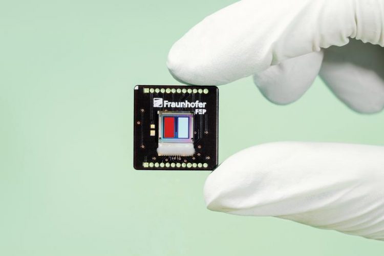
Prototype of the miniaturized phosphorescence sensor © Fraunhofer FEP, Photographer: Claudia Jacquemin | Picture in printable resolution: www.fep.fraunhofer.de/press
In the course of digitalization and increasingly comprehensive monitoring of processes, automated workflows, also in biomedical and environmental engineering, the range of choices in sensors is almost unlimited and they are increasingly adapted to the concrete application.
The right combination of parameters must be found, depending on the requirements such as the substance or object to be detected, the excitation and reaction time, the sensitivity range, the connection type, overall system configuration, and service life.
Considering just oxygen sensors, there are many current-based sensors on the market able to cover large temperature ranges, but they are difficult to miniaturize and restricted to certain measurement points.
Optical sensors, such as phosphorescence sensors, overcome these hurdles. They are popular alternatives due to their ease of handling and capability of being integrated into existing systems. The reliability, low susceptibility to interference, and simple maintenance of most devices quickly persuades users.
The Fraunhofer FEP has many years of expertise in the development and manufacture of highly integrated OLED-on-silicon electro-optical devices. This has become standard for realizing high-resolution microdisplays in Augmented- and Virtual-reality glasses, and is now increasingly under development for optical sensor solutions.
Optical fingerprint sensors have already been created by merging the display and image sensor into a so-called a bi-directional OLED microdisplay. In addition to the display function, the display pixels serve as smart illumination of the finger on the surface, whose features are then detected by the embedded photodiodes.
Now the researchers have taken another step and developed a miniaturized phosphorescence sensor. In this sensor, a chemical marker is excited by modulated blue OLED light. The phosphorescent response of the marker is then detected directly inside the sensor chip. The marker determines the substance to be measured; a typical application is measurement of an oxygen concentration.
Why not use commercial sensors? The challenge lays in the design of an extremely small sensor that combines all the functionalities and could be manufactured cost-effectively in future due to its small size. For this purpose, the OLED control and the sensor front-end were integrated into the silicon chip, then different configurations of the excitation and detection areas were investigated.
In the first stage, a miniaturized phosphorescence sensor was developed. This is barely the size of a thumbnail and combines the marker and sensor in a single component. It consists of a blue OLED integrated together with a commercially available marker on the silicon chip.
”Currently, the sensor is designed to detect changes in oxygen level. We have achieved functional verification of the component with this first setup, and can use the miniaturized sensor chip for oxygen measurements in gaseous environments.
In addition, we see the sensor chip as a platform for future developments, such as the measurement of further parameters and deployment in other environmental conditions,” explains Dr. Karsten Fehse, project manager in the Organic Microelectronic Devices group.
The current sensor emits blue light in an area of approx. 4.7 × 2.2 mm for exciting the oxygen-sensitive marker. The decay time of the light emitted by the marker after excitation is a parameter of the oxygen concentration of the environment. The significantly lower phosphorescence signal is recorded via integrated silicon photodiodes, amplified locally in the chip and subsequently evaluated in relation to the excitation signal with regard to the phase shift. In the future, the chip will be significantly reduced in size, the goal being <2 × 2 mm total chip size.
Thanks to the advantages of the innovative phosphorescence sensor – the small size, the combination of marker and sensor on a single chip, as well as the fast and precise evaluation of the data – the researchers see further areas of application in which the sensor design could be used.
The monitoring and evaluation of cell cultures in very small disposable culture vessels and in bioreactors is an interesting application example for the technology. ”Single-use bioreactors” usually only offer a very small installation space and a limited number of ports to which measurement systems can be connected. In the future, the sensor system will be further developed in the direction of multi-parameter measurements. Monitoring liquids after the filling process in the pharmaceutical sector, in blister packs, and for quality control of oxygen-sensitive drugs is also conceivable. The Fraunhofer FEP is very interested in project partnerships for these advanced developments.
Scientists of the Fraunhofer FEP will debut the miniaturized phosphorescence sensor for oxygen measurement at embedded world 2019, February 26 – 28 in Nuremberg at the Fraunhofer Joint Booth in Hall 4, Booth no. 4-470.
Press contact:
Ms. Annett Arnold
Fraunhofer Institute for Organic Electronics, Electron Beam and Plasma Technology FEP
Phone +49 351 2586 333 | presse@fep.fraunhofer.de
Winterbergstraße 28 | 01277 Dresden | Germany | www.fep.fraunhofer.de
Media Contact
All latest news from the category: Power and Electrical Engineering
This topic covers issues related to energy generation, conversion, transportation and consumption and how the industry is addressing the challenge of energy efficiency in general.
innovations-report provides in-depth and informative reports and articles on subjects ranging from wind energy, fuel cell technology, solar energy, geothermal energy, petroleum, gas, nuclear engineering, alternative energy and energy efficiency to fusion, hydrogen and superconductor technologies.


Newest articles
Combatting disruptive ‘noise’ in quantum communication
In a significant milestone for quantum communication technology, an experiment has demonstrated how networks can be leveraged to combat disruptive ‘noise’ in quantum communications. The international effort led by researchers…
Stretchable quantum dot display
Intrinsically stretchable quantum dot-based light-emitting diodes achieved record-breaking performance. A team of South Korean scientists led by Professor KIM Dae-Hyeong of the Center for Nanoparticle Research within the Institute for…

Internet can achieve quantum speed with light saved as sound
Researchers at the University of Copenhagen’s Niels Bohr Institute have developed a new way to create quantum memory: A small drum can store data sent with light in its sonic…

