Ultrafast optical switching can save overwhelmed datacenters
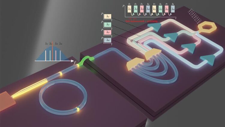
An illustration of photonic integrated platform that enables the ultrafast optical circuit switching for datacenters.
Credit: Aqeel Ahmed/EPFL
Services from all hyper-scale cloud providers like Microsoft are powered by massive datacenters that employ hundreds of thousands of servers, whose performance depends heavily on the quality of the network between them. Current datacenter networks include multiple layers of electrical packet switches interconnected through optical fibers.
These systems require electrical-to-optical conversion, which increases cost and power overhead. To make things worse, growing data rates due to applications like AI and data analytics could concur with the slowdown of Moore’s law which would make it extremely difficult to efficiently scale current network architectures relying on electrical chips.
Optical circuit switches (OCS) are emerging as an exciting option for overcoming bandwidth and scaling issues at datacenters. A particularly promising OCS architecture is wavelength switching where different servers are connected using different colors (wavelengths) of light leading to flatter network architecture and limiting the need for electrical switches and optical transceivers. Switching different wavelengths of light and routing signals to destination servers is done by a switching element, e.g. a glass prism through which different wavelengths can be separated by dispersion.
Although OCS technologies are commercially available today, they are extremely slow, which means they cannot handle increasingly bursty datacenter applications while properly utilizing network resources to reduce overheads and improve power consumption.
In a new paper published in Nature Communications, research teams led by Professor Tobias J. Kippenberg at EPFL and by Dr Hitesh Ballani at Microsoft Research Cambridge have successfully demonstrated ultrafast OCS for datacenters by using chip-based optics. The research teams have collaborated since 2018 as part of the Microsoft Swiss Joint Research Center.
In the proposed architecture, optical microcombs act as a multiwavelength source providing coherent carriers. Optical amplifiers and arrayed waveguide gratings based on semiconductor materials perform the switching and separate or combine the different colors of light respectively.
Optical microcombs, pioneered by Kippenberg’s group, provide hundreds of equidistantly spaced carriers that are suitable for many applications. The microcomb sources are generated through nonlinear frequency-conversion by using a chip-scale silicon nitride microresonator, presenting unique advantages in power and size over the laser arrays conventionally used as multi-wavelength sources.
Silicon nitride microresonators are fabricated using the photonic damascene process, a CMOS-compatible technique that features ultra-low propagation loss, which is extremely critical to make power-efficient microcomb sources.
The chip-scale indium phosphide-based optical amplifiers, fabricated using commercial foundries, perform the switching between different colors of light at sub-nanosecond timescales. This ultra-fast switching between different microcomb carriers is important for meeting the performance requirements of modern and future datacenter applications.
A proof-of-concept, system-level demonstration showed that data transmission with packet-by-packet switching can be achieved and hence, has the potential to meet the requirements of datacenter applications. Finally, the researchers present a unique architecture that employs a central comb system to improve power efficiency and reduce complexity.
“Soliton microcombs have been used in many key system-level applications such as LiDAR, long-haul data transmission, and optical coherence tomography since their discovery back in 2014,” says Kippenberg. “The potential use of microcombs in datacenters to meet future bandwidth requirements and reduce power consumption further consolidate the importance of this platform for scientific and technological applications.”
The silicon nitride samples were fabricated and grown in the Center of MicroNanoTechnology (CMi) at EPFL.
Funding
- Microsoft Swiss Joint Research Center (Joint research ICES)
- Air Force Office of Scientific Research (AFOSR)
- Swiss National Science Foundation (SNF)
- EU H2020
Reference
Arslan Sajid Raja, Sophie Lange, Maxim Karpov, Kai Shi, Xin Fu, Raphael Behrendt, Daniel Cletheroe, Anton Lukashchuk, Istvan Haller, Fotini Karinou, Benn Thomsen, Krzysztof Jozwik, Junqiu Liu, Paolo Costa, Tobias Jan Kippenberg, Hitesh Ballani. Ultrafast optical circuit switching for data centers using integrated soliton microcombs. Nature Communications 15 October 2021. DOI: 10.1038/s41467-021-25841-8
Contacts
Professor Tobias J. Kippenberg
+41 21 69 34428, +41 21 69 34452
tobias.kippenberg@epfl.ch
Dr Hitesh Ballani
+44 1223 479876
hitesh.ballani@microsoft.com
Arslan Sajid Raja
arslan.raja@epfl.ch
Journal: Nature Communications
DOI: 10.1038/s41467-021-25841-8
Method of Research: Experimental study
Article Title: Ultrafast optical circuit switching for data centers using integrated soliton microcombs.
Article Publication Date: 15-Oct-2021
Media Contact
Nik Papageorgiou
Ecole Polytechnique Fédérale de Lausanne
n.papageorgiou@epfl.ch
Office: 41-216-932-105
All latest news from the category: Physics and Astronomy
This area deals with the fundamental laws and building blocks of nature and how they interact, the properties and the behavior of matter, and research into space and time and their structures.
innovations-report provides in-depth reports and articles on subjects such as astrophysics, laser technologies, nuclear, quantum, particle and solid-state physics, nanotechnologies, planetary research and findings (Mars, Venus) and developments related to the Hubble Telescope.


Newest articles

Silicon Carbide Innovation Alliance to drive industrial-scale semiconductor work
Known for its ability to withstand extreme environments and high voltages, silicon carbide (SiC) is a semiconducting material made up of silicon and carbon atoms arranged into crystals that is…

New SPECT/CT technique shows impressive biomarker identification
…offers increased access for prostate cancer patients. A novel SPECT/CT acquisition method can accurately detect radiopharmaceutical biodistribution in a convenient manner for prostate cancer patients, opening the door for more…

How 3D printers can give robots a soft touch
Soft skin coverings and touch sensors have emerged as a promising feature for robots that are both safer and more intuitive for human interaction, but they are expensive and difficult…

