Guiding light – CMD19/CMMP with The Physics Congress 2002

A new type of optical material has been developed by physicists that could replace the electronics used to route the light signals through optical fibre telecommunications networks. It could even provide the basis for future `optical computers` working on light pulses instead of electric signals. At the Condensed Matter conference on Monday 8 April, part of the Institute of Physics Congress in Brighton, Dr David Sharp, a member of Dr Andrew Turberfield`s research team from the University of Oxford, will describe how they create these photonic crystals (optical equivalents of semiconductors) using a technique known as holographic lithography.
When separate beams of light meet each other, they either interfere constructively (adding together and becoming brighter) or destructively (cancelling each other out). In holographic lithography, four laser beams are arranged so as to produce a three-dimensional interference pattern of light and dark regions that represents the shape of the photonic crystal.
These laser beams are shone into a layer of almost transparent light-reactive polymer, so that the interference pattern is produced inside it. In any regions where constructive interference is taking place, and the light is therefore bright, a chemical change takes place in the polymer making that part of it insoluble (unable to be dissolved in a solvent). In the dark regions of the interference pattern however, where the light has been cancelled out, the polymer structure remains unchanged. As these unchanged parts are soluble, a solvent is used to wash them away, leaving behind the required photonic crystal structure.
Like photonic crystals made by other methods, the resulting crystals only let certain wavelengths (colours) of light pass through them. This quality is in itself useful, but “the big promise is that you can make miniaturised optical devices within these crystals,” says Dr Turberfield.
Being three-dimensional gives the Oxford team`s photonic crystals certain advantages over many of the other photonic crystals currently being created, which tend to be two-dimensional.
“One advantage is that it gives you a lot more scope for tighter integration. A 3D device architecture means you could pack things much more densely,” says Turberfield. Photonic crystals can act like an optical version of an electrical insulator, so a 3D structure would also reduce the amount of light lost from any optical devices built inside it because it would prevent the light from escaping through it in any direction.
Although he doesn`t rule out optical computers based on photonic crystals as a possibility sometime in the future, “more realistic applications would be in passive optical processing devices, such as those used now in telecomms for routing,” says Turberfield. As data is sent down optical fibres in the form of pulses of light, using such devices for routing would make telecommunications networks more efficient. Whenever data reached a junction in the network, it would be processed as light instead of being converted from light into an electronic signal, then back into light again, before being sent down the correct pathway.
Media Contact
All latest news from the category: Physics and Astronomy
This area deals with the fundamental laws and building blocks of nature and how they interact, the properties and the behavior of matter, and research into space and time and their structures.
innovations-report provides in-depth reports and articles on subjects such as astrophysics, laser technologies, nuclear, quantum, particle and solid-state physics, nanotechnologies, planetary research and findings (Mars, Venus) and developments related to the Hubble Telescope.
Newest articles
A new look at the consequences of light pollution
GAME 2024 begins its experiments in eight countries. Can artificial light at night harm marine algae and impair their important functions for coastal ecosystems? This year’s project of the training…
Silicon Carbide Innovation Alliance to drive industrial-scale semiconductor work
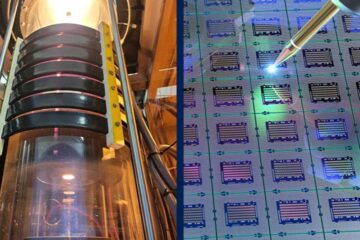
Known for its ability to withstand extreme environments and high voltages, silicon carbide (SiC) is a semiconducting material made up of silicon and carbon atoms arranged into crystals that is…
New SPECT/CT technique shows impressive biomarker identification
…offers increased access for prostate cancer patients. A novel SPECT/CT acquisition method can accurately detect radiopharmaceutical biodistribution in a convenient manner for prostate cancer patients, opening the door for more…


