Intelligent nanomaterials for photonics
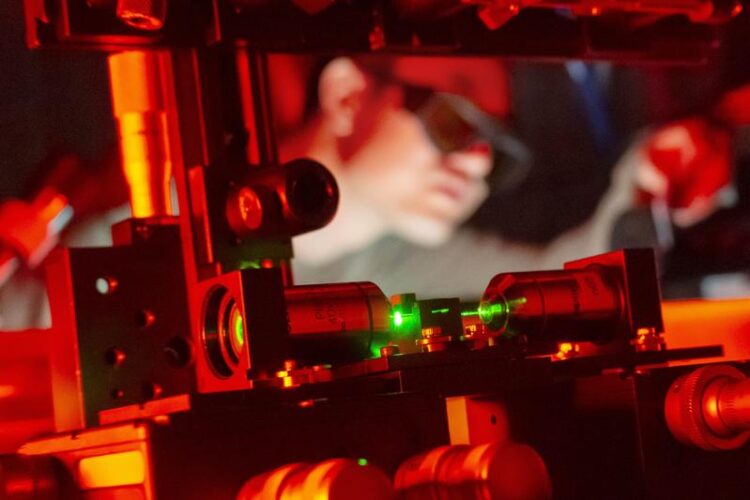
PhD student Quyet Ngo studies optical fibres functionalised by 2D materials.
Jens Meyer/Uni Jena
2D materials – nanosheets with atomic thickness – have enormous potential for a wide variety of applications. For instance, combined with optical fibres, 2D materials can enable novel applications in the areas of sensors, non-linear optics, and quantum technologies. However, combining these two components has so far been very laborious. Typically, the atomically thin layers had to be produced separately before being transferred by hand onto the optical fibre. Together with Australian colleagues, Jena researchers have now succeeded for the first time in growing 2D materials directly on optical fibres. This approach significantly facilitates manufacturing of such hybrids.
“We integrated transition metal dichalcogenides – a 2D material with excellent optical and photonic properties, which, for example, interacts strongly with light – into specially developed glass fibres,” explains Dr Falk Eilenberger of the University of Jena and the Fraunhofer Institute for Applied Optics and Precision Engineering (IOF) in Germany.
“Unlike in the past, we did not apply the half-nanometre-thick sheet manually, but grew it directly on the fibre,” says Eilenberger, a specialist in the field of nanophotonics. “This improvement means that the 2D material can be integrated into the fibre more easily and on a large scale. We were also able to show that the light in the glass fibre strongly interacts with its coating.” The step to a practical application for the intelligent nanomaterial thus created is no longer very far away.
The success has been achieved thanks to a growth process developed at the Institute of Physical Chemistry of the University of Jena, which overcomes previous hurdles. “By analysing and controlling the growth parameters, we identified the conditions at which the 2D material can directly grow in the fibres,” says Jena 2D materials expert Prof. Andrey Turchanin, explaining the method based on chemical vapour deposition (CVD) techniques. Among other things, a temperature of over 700 degrees Celsius is necessary for the 2D material growth.
Hybrid material platform
Despite this high temperature, the optical fibres can be used for the direct CVD growth: “The pure quartz glass that serves as the substrate withstands the high temperatures extremely well. It is heat-resistant up to 2,000 degrees Celsius,” says Prof. Markus A. Schmidt of the Leibniz Institute of Photonic Technology, who developed the fibres. “Their small diameter and flexibility enable a variety of applications,” adds Schmidt, who also holds an endowed professorship for fibre optics at the University of Jena.
The combination of 2D material and glass fibre has thus created an intelligent material platform that combines the best of both worlds. “Due to the functionalisation of the glass fibre with the 2D material, the interaction length between light and material has now been significantly increased,” says Dr Antony George, who is developing the manufacturing method for the novel 2D materials together with Turchanin.
Sensors and non-linear light converters
The team envisages potential applications for the newly developed materials system in two particular areas. Firstly, the materials combination is very promising for sensor technology. It could be used, for example, to detect low concentrations of gases. To this end, a green light sent through the fibre picks up information from the environment at the fibre areas functionalised with the 2D material. As external influences change the fluorescent properties of the 2D material, the light changes colour and returns to a measuring device as red light. Since the fibres are very fine, sensors based on this technology might also be suitable for applications in biotechnology or medicine.
Secondly, such a system could also be used as a non-linear light converter. Due to its non-linear properties, the hybrid optical fibre can be employed to convert a monochromatic laser light into white light for spectroscopy applications in biology and chemistry. The Jena researchers also envisage applications in the areas of quantum electronics and quantum communication.
Exceptional interdisciplinary cooperation
The scientists involved in this development emphasise that the success of the project was primarily due to the exceptional interdisciplinary cooperation between various research institutes in Jena. Based on the Thuringian research group “2D-Sens” and the Collaborative Research Centre “Nonlinear Optics down to Atomic Scales” of Friedrich Schiller University, experts from the Institute of Applied Physics and Institute of Physical Chemistry of the University of Jena; the University’s Abbe Center of Photonics; the Fraunhofer Institute for Applied Optics and Precision Engineering IOF; and the Leibniz Institute of Photonic Technology are collaborating on this research, together with colleagues in Australia.
“We have brought diverse expertise to this project and we are delighted with the results achieved,” says Eilenberger. “We are convinced that the technology we have developed will further strengthen the state of Thuringia as an industrial centre with its focus on photonics and optoelectronics,” adds Turchanin. A patent application for the interdisciplinary team’s invention has recently been filed.
Wissenschaftliche Ansprechpartner:
Dr Falk Eilenberger
Institute of Applied Physics of Friedrich Schiller University Jena
Albert-Einstein-Straße 15, 07745 Jena, Germany
Tel.: +49 (0)3641/947990
E-mail: falk.eilenberger[at]uni-jena.de
Prof. Dr Andrey Turchanin
Institute of Physical Chemistry of Friedrich Schiller University Jena
Lessingstr. 10, 07743 Jena, Germany
Tel.: +49 (0)3641/948370
E-mail: andrey.turchanin[at]uni-jena.de
Originalpublikation:
G. Quyet Ngo, A. George, R. T. K. Schock, A. Tuniz, E. Najafidehaghani, Z. Gan, N. C. Geib, T. Bucher, H. Knopf, S. Saravi, Chr. Neumann, T. Lühder, E. P. Schartner, S. C. Warren-Smith, H. Ebendorff-Heidepriem, Th. Pertsch, Markus A. Schmidt, A. Turchanin, F. Eilenberger (2020): Scalable functionalization of optical fibers using atomically thin semiconductors, Advanced Materials, DOI: 10.1002/adma.202003826
Media Contact
All latest news from the category: Physics and Astronomy
This area deals with the fundamental laws and building blocks of nature and how they interact, the properties and the behavior of matter, and research into space and time and their structures.
innovations-report provides in-depth reports and articles on subjects such as astrophysics, laser technologies, nuclear, quantum, particle and solid-state physics, nanotechnologies, planetary research and findings (Mars, Venus) and developments related to the Hubble Telescope.


Newest articles

High-energy-density aqueous battery based on halogen multi-electron transfer
Traditional non-aqueous lithium-ion batteries have a high energy density, but their safety is compromised due to the flammable organic electrolytes they utilize. Aqueous batteries use water as the solvent for…

First-ever combined heart pump and pig kidney transplant
…gives new hope to patient with terminal illness. Surgeons at NYU Langone Health performed the first-ever combined mechanical heart pump and gene-edited pig kidney transplant surgery in a 54-year-old woman…

Biophysics: Testing how well biomarkers work
LMU researchers have developed a method to determine how reliably target proteins can be labeled using super-resolution fluorescence microscopy. Modern microscopy techniques make it possible to examine the inner workings…

