Upgrading your computer to quantum
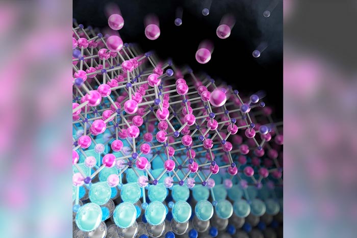
Researchers at The University of Tokyo grow a nanoscale layer of a superconducting material on top of a nitride-semiconductor substrate, which may help facilitate the integration of quantum qubits with existing microelectronics
Credit: Institute of Industrial Science, The University of Tokyo
Computers that can make use of the “spooky” properties of quantum mechanics to solve problems faster than current technology may sound alluring, but first they must overcome a massive disadvantage. Scientists from Japan may have found the answer through their demonstration of how a superconducting material, niobium nitride, can be added to a nitride-semiconductor substrate as a flat, crystalline layer. This process may lead to the easy manufacturing of quantum qubits connected with conventional computer devices.
The processes used to manufacture conventional silicon microprocessors have matured over decades and are constantly being refined and improved. In contrast, most quantum computing architectures must be designed mostly from scratch. However, finding a way to add quantum capabilities to existing fabrication lines, or even integrate quantum and conventional logic units in a single chip, might be able to vastly accelerate the adoption of these new systems.
Now, a team of researchers at the Institute of Industrial Science at The University of Tokyo have shown how thin films of niobium nitride (NbNx) can be grown directly on top of an aluminum nitride (AlN) layer. Niobium nitride can become superconducting at temperatures colder than about 16 degrees above absolute zero. As a result, it can be used to make a superconducting qubit when arranged in a structure called a Josephson junction. The scientists investigated the impact of temperature on the crystal structures and electrical properties of NbNx thin films grown on AlN template substrates. They showed that the spacing of atoms in the two materials was compatible enough to produce flat layers. “We found that because of the small lattice mismatch between aluminum nitride and niobium nitride, a highly crystalline layer could grow at the interface,” says first and corresponding author Atsushi Kobayashi.
The crystallinity of the NbNx was characterized with X-ray diffraction, and the surface topology was captured using atomic force microscopy. In addition, the chemical composition was checked using X-ray photoelectron spectroscopy. The team showed how the arrangement of atoms, nitrogen content, and electrical conductivity all depended on the growth conditions, especially the temperature. “The structural similarity between the two materials facilitates the integration of superconductors into semiconductor optoelectronic devices,” says Atsushi Kobayashi.
Moreover, the sharply defined interface between the AlN substrate, which has a wide bandgap, and NbNx, which is a superconductor, is essential for future quantum devices, such as Josephson junctions. Superconducting layers that are only a few nanometers thick and high crystallinity can be used as detectors of single photons or electrons.
The work is published in Advanced Materials Interfaces as “Crystal-phase controlled epitaxial growth of NbNx superconductors on wide-bandgap AlN semiconductors” (DOI: 10.1002/admi.202201244).
About Institute of Industrial Science, The University of Tokyo
The Institute of Industrial Science, The University of Tokyo (UTokyo-IIS) is one of the largest university-attached research institutes in Japan. UTokyo-IIS is comprised of over 120 research laboratories—each headed by a faculty member—and has over 1,200 members (approximately 400 staff and 800 students) actively engaged in education and research. Its activities cover almost all areas of engineering. Since its foundation in 1949, UTokyo-IIS has worked to bridge the huge gaps that exist between academic disciplines and real-world applications.
DOI: 10.1002/admi.202201244
Article Title: Advanced Materials Interfaces
Article Publication Date: 22-Sep-2022
Media Contact
KOBAYASHI Atsushi
Institute of Industrial Science, The University of Tokyo
akoba@iis.u-tokyo.ac.jp
Office: 81-354-526-344
Original Source
Media Contact
All latest news from the category: Materials Sciences
Materials management deals with the research, development, manufacturing and processing of raw and industrial materials. Key aspects here are biological and medical issues, which play an increasingly important role in this field.
innovations-report offers in-depth articles related to the development and application of materials and the structure and properties of new materials.


Newest articles

High-energy-density aqueous battery based on halogen multi-electron transfer
Traditional non-aqueous lithium-ion batteries have a high energy density, but their safety is compromised due to the flammable organic electrolytes they utilize. Aqueous batteries use water as the solvent for…

First-ever combined heart pump and pig kidney transplant
…gives new hope to patient with terminal illness. Surgeons at NYU Langone Health performed the first-ever combined mechanical heart pump and gene-edited pig kidney transplant surgery in a 54-year-old woman…

Biophysics: Testing how well biomarkers work
LMU researchers have developed a method to determine how reliably target proteins can be labeled using super-resolution fluorescence microscopy. Modern microscopy techniques make it possible to examine the inner workings…

