Unique ferroelectric microstructure revealed for first time
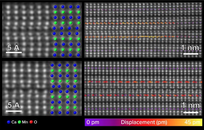
An atomically resolved scanning transmission electron microscopy (STEM) image of the polar nanoregions (PNRs) embedded in the nonpolar matrix in the layered perovskite material (Ca, Sr)3Mn2O7. Bright contrast in the images can be directly interpreted as the atomic columns in the crystal. Aberration corrected STEM was employed to direct capture the arrangement of the atoms in the (a-type and b-type) polar nanoregions in the crystal and the displacement measurement at picometer precision were performed on the STEM images to extract the distortion in the structure.
Credit: Alem Group/Jennifer M. McCann, MRI
A team of researchers have observed and reported for the first time the unique microstructure of a novel ferroelectric material, enabling the development of lead-free piezoelectric materials for electronics, sensors, and energy storage that are safer for human use. This work was led by the Alem Group at Penn State and in collaboration with research teams at Rutgers University and the University of California, Merced.
Ferroelectrics are a class of materials that demonstrate a spontaneous electric polarization when an external electric charge is applied. This causes a spontaneous electric polarization when positive and negative charges in the materials head to different poles. These materials also have piezoelectric properties, which means the material generates an electrical charge under an applied mechanical force.
This enables these materials to make electricity from energy like heat, movement, or even noise that might otherwise be wasted. Therefore, they hold potential for alternatives to carbon-based energy, such as harvesting energy from waste heat. In addition, ferroelectric materials are especially useful for data storage and memory as they can remain in one polarized state without additional power, making them attractive for energy-saving data storage and electronics. They are also widely used in beneficial applications such as switches, important medical devices like heart-rate monitors and ultrasounds, energy storage and actuators.
However, the strongest piezoelectric materials contain lead, which is a major issue given lead is toxic for humans and animals.
“We would love to design a piezoelectric material that doesn’t have the disadvantages of the current materials,” Nasim Alem, Penn State associate professor of materials science and engineering and the study’s corresponding author, said. “And right now, lead in all these materials is a big disadvantage because the lead is hazardous. We hope that our study can result in a suitable candidate for a better piezoelectric system.”
To develop a pathway to such a lead-free material with strong piezoelectric properties, the research team worked with calcium manganate, Ca3Mn2O7 (CMO). CMO is a novel hybrid improper ferroelectric material with some interesting properties.
“The designing principle of this material is combining the motion of the material’s little oxygen octahedra,” said Leixin Miao, doctoral candidate in materials science and first author of the study in Nature Communications. “In the material, there are octahedra of oxygen atoms that can tilt and rotate. The term ‘hybrid improper ferroelectric’ means we combine the rotation and the tilting of the octahedra to produce ferroelectricity. It is considered a ‘hybrid’ because it is the combination of two motions of the octahedra generating that polarization for ferroelectricity. It is considered an ‘improper’ ferroelectric since the polarization is generated as a secondary effect.”
There is also a unique characteristic of CMO’s microstructure that is something of a mystery to researchers.
“At room temperature, there are some polar and nonpolar phases coexisting at room temperature in the crystal,” Miao said. “And those coexisting phases are believed to be correlated with negative thermal expansion behavior. It is well-known that normally, a material expands when heated, but this one shrinks. That is interesting, but we know very little about the structure, like how the polar and nonpolar phases coexist.”
To better understand this, the researchers used atomic-scale transmission electron microscopy.
“Why we used electron microscopy is because with electron microscopy, we can use atomic-scale probes to see the exact atomic arrangement in the structure,” Miao said. “And it was very surprising to observe the double bilayer polar nanoregions in the CMO crystals. To our knowledge, it is the first time that such microstructure was directly imaged in the layered perovskite materials.”
Before, it was never observed what happens to a material that goes through such a ferroelectric phase transition, according to the researchers. But with electron microscopy, they could monitor the material and what was happening during the phase transition.
“We monitored the material, what’s going on during the phase transition, and were able to probe atom by atom at what type of bonding we have, what type of structural distortions we have in the material, and how that may change as a function of temperature,” Alem said. “And this is very much explaining some of the observations that people have had with this material. For example, when they get the thermal expansion coefficient, no one has really known where this comes from. Basically, this was going down into the atomic level and understanding the underlying atomic-scale physics, chemistry and also the phase transition’s dynamics, how it’s changing.”
This in turn would enable the development of lead-free, powerful piezoelectric materials.
“Scientists have been trying to find new paths to discover lead-free ferroelectric materials for many beneficial applications,” Miao said. “The existence of the polar nanoregions is considered to benefit the piezoelectric properties, and now we showed that via defect engineering, we may be able to design new strong piezoelectric crystals that would ultimately replace all lead containing materials for ultrasonic or actuator applications.”
The characterization work that revealed these never-before-seen processes in the material was carried out at the Materials Research Institute’s facilities in the Millennium Science Complex. This included multiple transmission electron microscopes (TEM) experiments that enabled the never-before-seen to be seen.
Another benefit of the study was free software developed by the research team, EASY-STEM, that enables easier TEM image data processing. This could potentially shorten the time needed to advance scientific research and move it to practical application.
“The software has a graphical user interface that allows users to input with mouse clicks, so people do not need to be an expert in coding but still can generate amazing analysis,” Miao said.
Along with Miao and Alem, other authors of the study include from Penn State Parivash Moradifar, doctoral candidate at the time, and Ke Wang, staff scientist with MRI. From the University of California, authors include Kishwar-E Hasin, graduate student in computational materials science and simulation and Elizabeth A. Nowadnick, assistant professor of materials science and engineering. Additional authors include from Oak Ridge National Laboratory Debangshu Mukherjee, R&D associate scientist, and from Rutgers University Sang-Wook Cheong, distinguished professor, Henry Rutgers Professor, Board of Governors Professor and director, Center for Quantum Materials Synthesis.
The study was supported by the National Science Foundation.
Journal: Nature Communications
DOI: 10.1038/s41467-022-32090-w
Method of Research: Experimental study
Subject of Research: Not applicable
Article Title: Double-Bilayer polar nanoregions and Mn antisites in (Ca, Sr)3Mn2O7
Article Publication Date: 22-Aug-2022
Media Contact
Adrienne Berard
Penn State
akb6884@psu.edu
All latest news from the category: Materials Sciences
Materials management deals with the research, development, manufacturing and processing of raw and industrial materials. Key aspects here are biological and medical issues, which play an increasingly important role in this field.
innovations-report offers in-depth articles related to the development and application of materials and the structure and properties of new materials.


Newest articles

Silicon Carbide Innovation Alliance to drive industrial-scale semiconductor work
Known for its ability to withstand extreme environments and high voltages, silicon carbide (SiC) is a semiconducting material made up of silicon and carbon atoms arranged into crystals that is…

New SPECT/CT technique shows impressive biomarker identification
…offers increased access for prostate cancer patients. A novel SPECT/CT acquisition method can accurately detect radiopharmaceutical biodistribution in a convenient manner for prostate cancer patients, opening the door for more…

How 3D printers can give robots a soft touch
Soft skin coverings and touch sensors have emerged as a promising feature for robots that are both safer and more intuitive for human interaction, but they are expensive and difficult…

