The photoexcited graphene puzzle solved
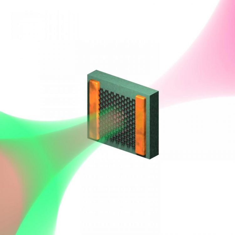
Schematic representation of the ultrafast optical pump - terahertz probe experiment, where the optical pump induces electron heating and the terahertz pulse is sensitive to the conductivity of graphene directly after this heating process, which occurs on a timescale faster than a millionth of a millionth of a second Credit: Illustration: Fabien Vialla/ICFO
Light detection and control lies at the heart of many modern device applications, such as the camera you have in your phone. Using graphene as a light-sensitive material for light detectors can offer significant improvements with respect to materials being used nowadays.
For example, graphene can detect light of almost any colour, and it gives an extremely fast electronic response within one millionth of a millionth of a second. Thus, in order to properly design graphene-based light detectors it is crucial to understand the processes that take place inside the graphene after it absorbs light.
A team of European scientists including ICFO from Barcelona (Spain), IIT from Genova (Italy), the University of Exeter from Exeter (UK) and Johannes Gutenberg University from Mainz (Germany), have now succeeded in understanding these processes.
Published recently in Science Advances, their work gives a thorough explanation of why, in some cases, the graphene conductivity increases after light absorption and in other cases, it decreases. The researchers show that this behaviour correlates with the way in which energy from absorbed light flows to the graphene electrons: After light is absorbed by the graphene, the processes through which graphene electrons heat up happen extremely fast and with a very high efficiency.
For highly doped graphene (where many free electrons are present), ultrafast electron heating leads to carriers with elevated energy – hot carriers – which, in turn, leads to a decrease in conductivity. Interestingly enough, for weakly doped graphene (where not so many free electrons are present), electron heating leads to the creation of additional free electrons, and therefore an increase in conductivity. These additional carriers are the direct result of the gapless nature of graphene – in gapped materials, electron heating does not lead to additional free carriers.
This simple scenario of light-induced electron heating in graphene can explain many observed effects. Aside from describing the conductive properties of the material after light absorption, it can explain carrier multiplication, where – under specific conditions – one absorbed light particle (photon) can indirectly generate more than one additional free electron, and thus create an efficient photoresponse within a device.
The results of the paper, in particular, understanding electron heating processes accurately, will definitely mean a great boost in the design and development of graphene-based light detection technology.
###
This work was funded by the E.C. under Graphene Flagship, as well as a Mineco Young Investigator grant.
Media Contact
All latest news from the category: Materials Sciences
Materials management deals with the research, development, manufacturing and processing of raw and industrial materials. Key aspects here are biological and medical issues, which play an increasingly important role in this field.
innovations-report offers in-depth articles related to the development and application of materials and the structure and properties of new materials.


Newest articles
Machine learning algorithm reveals long-theorized glass phase in crystal
Scientists have found evidence of an elusive, glassy phase of matter that emerges when a crystal’s perfect internal pattern is disrupted. X-ray technology and machine learning converge to shed light…
Mapping plant functional diversity from space
HKU ecologists revolutionize ecosystem monitoring with novel field-satellite integration. An international team of researchers, led by Professor Jin WU from the School of Biological Sciences at The University of Hong…
Inverters with constant full load capability
…enable an increase in the performance of electric drives. Overheating components significantly limit the performance of drivetrains in electric vehicles. Inverters in particular are subject to a high thermal load,…

