Just a few atoms thick: New functional materials developed
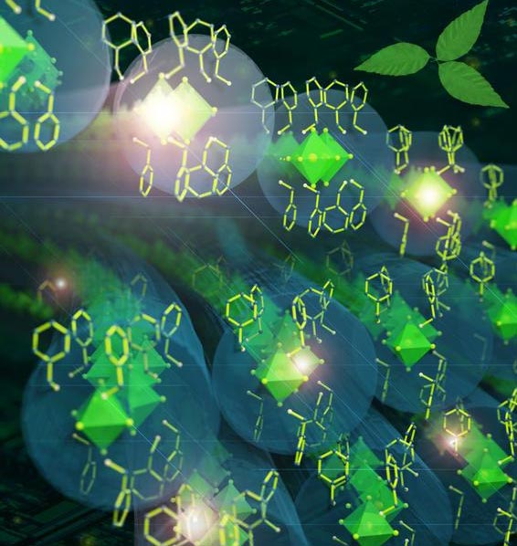
Artistic representation of the crystal structure of the innovative material. Individual layers of the crystal can simply be lifted off.
Credit: Elisa Monte, Experimental Physics I, Justus Liebig University of Giessen
Using the smallest “construction set” in the world, a research team from the universities of Marburg, Giessen and Paderborn is designing new materials for computer chips, light-emitting diodes and solar cells.
They are 50,000 times thinner than a human hair, and just a few atoms thick: two-dimensional materials are the thinnest substances it is possible to make today. They have completely new properties and are regarded as the next major step in modern semiconductor technology.
In the future they could be used instead of silicon in computer chips, light-emitting diodes and solar cells. Until now, the development of new two-dimensional materials has been limited to structures with layers of rigid chemical bonds in two spatial directions – like a sheet of paper in a stack. Now for the first time, a research team from the universities of Marburg, Giessen and Paderborn, led by Dr. Johanna Heine (Inorganic Chemistry, Philipps University of Marburg) has overcome this limitation by using an innovative concept.
The researchers developed an organic-inorganic hybrid crystal which consists of chains in a single direction, yet still forms two-dimensional layers in spite of this. This makes it possible to combine different material components, like pieces in a construction set, to create tailored materials with innovative properties.
In this project, the research team combined the advantages of two-dimensional materials and hybrid perovskites – the eponymous mineral perovskite is well-known for its optoelectronic properties, and can be combined with other materials to improve these characteristics. “What is special about this is that it offers completely new options for targeted design of future functional materials,” says Dr. Johanna Heine, a chemist and junior research group leader at the University of Marburg, describing this highly topical research area which has great application potential.
“This physical effect – first discovered here – could make it possible to tune the colour of future lighting and display technologies in a simple and targeted way,” says physicist Philip Klement, lead author and doctoral student in the research group led by Professor Sangam Chatterjee at the Justus Liebig University of Giessen (JLU).
The work was carried out in an interdisciplinary collaboration: Dr. Johanna Heine’s team at the University of Marburg first developed the chemical synthesis and created the material as a single bulk crystal. Philip Klement and Professor Chatterjee’s team at JLU then used these crystals to produce individual atomically thin layers and investigated them using optical laser spectroscopy. They found a spectrally broadband (“white”) light emission, whose colour temperature can be tuned by changing the thickness of the layer. Working closely with Professor Stefan Schumacher and his team of theoretical physicists at Paderborn University the researchers made a microscopic study of the effect and were able to improve the properties of the material.
In this way the researchers were able to cover the entire process from synthesis of the material and understanding its properties, to modelling the properties. Their findings have been published in the specialist journal “Advanced Materials“.
###
Publication:
Philip Klement, Natalie Dehnhardt, Chuan-Ding Dong, Florian Dobener, Samuel Bayliff, Julius Winkler, Detlev M. Hofmann, Peter J. Klar, Stefan Schumacher, Sangam Chatterjee, and Johanna Heine: Atomically Thin Sheets of Lead-Free One-Dimensional Hybrid Perovskites Feature Tunable White-Light Emission from Self-Trapped Excitons. Advanced Materials 2021, https:/
All latest news from the category: Materials Sciences
Materials management deals with the research, development, manufacturing and processing of raw and industrial materials. Key aspects here are biological and medical issues, which play an increasingly important role in this field.
innovations-report offers in-depth articles related to the development and application of materials and the structure and properties of new materials.


Newest articles

Superradiant atoms could push the boundaries of how precisely time can be measured
Superradiant atoms can help us measure time more precisely than ever. In a new study, researchers from the University of Copenhagen present a new method for measuring the time interval,…

Ion thermoelectric conversion devices for near room temperature
The electrode sheet of the thermoelectric device consists of ionic hydrogel, which is sandwiched between the electrodes to form, and the Prussian blue on the electrode undergoes a redox reaction…

Zap Energy achieves 37-million-degree temperatures in a compact device
New publication reports record electron temperatures for a small-scale, sheared-flow-stabilized Z-pinch fusion device. In the nine decades since humans first produced fusion reactions, only a few fusion technologies have demonstrated…

