High-quality growth

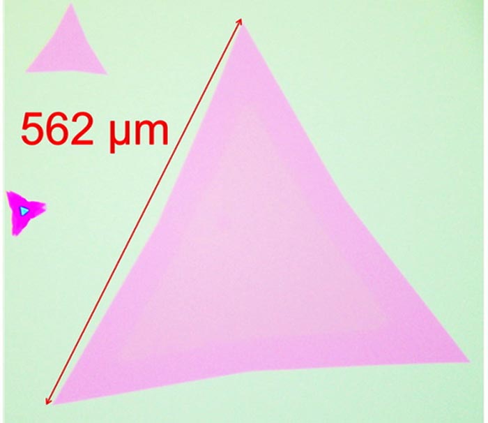
Optical micrograph of large size monolayer WS2 crystal.
Credit: Okayama University
Transition metal dichalcogenides (TMDCs) are a class of materials with physical properties that make them ideally suited for use in flexible optoelectronic applications, such as light detectors, light-emitting diodes and solar cells.
For such applications to perform well, the crystalline quality of the TMDCs needs to be extremely high, however; defects in the crystal structure worsen device performance. The crystalline quality of a sample is related to the number of grain boundaries — interfaces between different grains, or domains, within the crystal. Different domains have the same chemical composition and structure but are oriented differently with respect to each other.
The lower the number of grain boundaries, the larger the domains, and the better the sample’s crystallinity. Now, Assistant Professor SUZUKI Hiroo and HASHIMOTO Ryoki (graduate students) Okayama University and colleagues have developed a technique with which highly crystalline TMDCs can be grown. Furthermore, the technique enables to optimize the performance of TMDCs for optoelectronic devices.
The researchers’ approach is based on chemical vapor deposition (CVD), a method in which a substrate is put in a vacuum chamber and is exposed to particular chemical vapors. This leads to chemical reactions and depositions on the substrate, resulting in the growth of the desired material. Assistant Professor SUZUKI and colleagues grew the TMDCs MoS2 (molybdenum disulfide) and WS2 (tungsten disulfide), for which they let metal salts and sulfur sources react in the CVD chamber. What was special is that they used a stacked substrate configuration: two silicon-based substrates put close to each other, creating a confined environment for the TMDCs to form. This type of ‘microreactor’ led to the growth of samples with large domains.
Through careful analysis of the obtained crystals’ morphology and numerical modelling of the processes at play, Assistant Professor SUZUKI and colleagues deduced that the growth is governed by surface diffusion, that is, by atoms moving along the substrate surface. This leads to a lower probability for atoms to nucleate and initiate the growth of a domain; instead of several small domains, only one or a few large domains develop.
The scientists then investigated how the growth temperature used in the CVD process influenced the materials’ photoluminescence — the ability to emit light of a particular wavelength after being irradiated with light of another wavelength. They found that for a growth temperature of about 820°C, the photoluminescence characteristics of WS2 are optimal.
In conclusion, the reported growth method produces, in a controlled way, highly crystalline TMDC samples that are suitable for use in optoelectronic applications. Quoting the researchers: “These findings should significantly contribute to the realization of applications of high-performance optoelectronic devices based on high-quality monolayer TMDCs.”
Background
Chemical vapor deposition
In chemical vapor deposition (CVD), one or more gases are made to pass over a hot substrate’s surface under (low) vacuum. The gases dissociate on the substrate or in its immediate vicinity, after which the decomposition products accumulate on the surface. Often, by-products are formed in the process; these are removed from the reaction chamber through gas flow.
By choosing the gases that are injected into the CVD chamber, specific materials can be grown. Various types of materials structures can be obtained, including monocrystalline (consisting of one domain only), polycrystalline (consisting of several domains) or amorphous materials.
Assistant Professor SUZUKI Hiroo and HASHIMOTO Ryoki from Okayama University and colleagues have now used a CVD approach to grow highly crystalline samples of transition metal dichalcogenides, specifically MoS2 and WS2, by using a stacked substrate setup; the resulting confinement provides optimal conditions for monocrystals to grow.
Journal: ACS Nano
DOI: 10.1021/acsnano.2c05076
Article Title: Surface Diffusion-Limited Growth of Large and High-Quality Monolayer Transition Metal Dichalcogenides in Confined Space of Microreactor
Article Publication Date: 6-Jul-2022
Media Contact
Ryoko Mimura
Okayama University
mimura-r@adm.okayama-u.ac.jp
Original Source
All latest news from the category: Materials Sciences
Materials management deals with the research, development, manufacturing and processing of raw and industrial materials. Key aspects here are biological and medical issues, which play an increasingly important role in this field.
innovations-report offers in-depth articles related to the development and application of materials and the structure and properties of new materials.
Newest articles

“Nanostitches” enable lighter and tougher composite materials
In research that may lead to next-generation airplanes and spacecraft, MIT engineers used carbon nanotubes to prevent cracking in multilayered composites. To save on fuel and reduce aircraft emissions, engineers…

Trash to treasure
Researchers turn metal waste into catalyst for hydrogen. Scientists have found a way to transform metal waste into a highly efficient catalyst to make hydrogen from water, a discovery that…

Real-time detection of infectious disease viruses
… by searching for molecular fingerprinting. A research team consisting of Professor Kyoung-Duck Park and Taeyoung Moon and Huitae Joo, PhD candidates, from the Department of Physics at Pohang University…


