Connecting the (nano) dots: Big-picture thinking can advance nanoparticle manufacturing
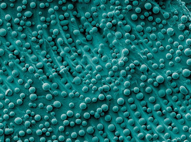
This is an electron micrograph showing gallium arsenide nanoparticles of varying shapes and sizes. Such heterogeneity can increase costs and limit profits when making nanoparticles into products. A new NIST study recommends that researchers, manufacturers and administrators work together to solve this, and other common problems, in nanoparticle manufacturing. Credit: A. Demotiere and E. Shevchenko/Argonne National Laboratory
To help overcome these obstacles, the National Institute of Standards and Technology (NIST) and the nonprofit World Technology Evaluation Center (WTEC) advocate that nanoparticle researchers, manufacturers and administrators “connect the dots” by considering their shared challenges broadly and tackling them collectively rather than individually. This includes transferring knowledge across disciplines, coordinating actions between organizations and sharing resources to facilitate solutions.
The recommendations are presented in a new paper in the journal ACS Applied Nano Materials.
“We looked at the big picture of nanoparticle manufacturing to identify problems that are common for different materials, processes and applications,” said NIST physical scientist Samuel Stavis, lead author of the paper. “Solving these problems could advance the entire enterprise.”
The new paper provides a framework to better understand these issues. It is the culmination of a study initiated by a workshop organized by NIST that focused on the fundamental challenge of reducing or mitigating heterogeneity, the inadvertent variations in nanoparticle size, shape and other characteristics that occur during their manufacture.
“Heterogeneity can have significant consequences in nanoparticle manufacturing,” said NIST chemical engineer and co-author Jeffrey Fagan.
In their paper, the authors noted that the most profitable innovations in nanoparticle manufacturing minimize heterogeneity during the early stages of the operation, reducing the need for subsequent processing. This decreases waste, simplifies characterization and improves the integration of nanoparticles into products, all of which save money.
The authors illustrated the point by comparing the production of gold nanoparticles and carbon nanotubes. For gold, they stated, the initial synthesis costs can be high, but the similarity of the nanoparticles produced requires less purification and characterization. Therefore, they can be made into a variety of products, such as sensors, at relatively low costs.
In contrast, the more heterogeneous carbon nanotubes are less expensive to synthesize but require more processing to yield those with desired properties. The added costs during manufacturing currently make nanotubes only practical for high-value applications such as digital logic devices.
“Although these nanoparticles and their end products are very different, the stakeholders in their manufacture can learn much from each other's best practices,” said NIST materials scientist and co-author J. Alexander Liddle. “By sharing knowledge, they might be able to improve both seemingly disparate operations.”
Finding ways like this to connect the dots, the authors said, is critically important for new ventures seeking to transfer nanoparticle technologies from laboratory to market.
“Nanoparticle manufacturing can become so costly that funding expires before the end product can be commercialized,” said WTEC nanotechnology consultant and co-author Michael Stopa. “In our paper, we outlined several opportunities for improving the odds that new ventures will survive their journeys through this technology transfer 'valley of death.'”
Finally, the authors considered how manufacturing challenges and innovations are affecting the ever-growing number of applications for nanoparticles, including those in the areas of electronics, energy, health care and materials.
###
Paper: S.M. Stavis, J.A. Fagan, M. Stopa and J.A. Liddle. Nanoparticle manufacturing–heterogeneity through processes to products. ACS Applied Nano Materials, August 2018. DOI: 10.1021/acsanm.8b01239
Media Contact
More Information:
http://dx.doi.org/10.1021/acsanm.8b01239All latest news from the category: Materials Sciences
Materials management deals with the research, development, manufacturing and processing of raw and industrial materials. Key aspects here are biological and medical issues, which play an increasingly important role in this field.
innovations-report offers in-depth articles related to the development and application of materials and the structure and properties of new materials.


Newest articles

Silicon Carbide Innovation Alliance to drive industrial-scale semiconductor work
Known for its ability to withstand extreme environments and high voltages, silicon carbide (SiC) is a semiconducting material made up of silicon and carbon atoms arranged into crystals that is…

New SPECT/CT technique shows impressive biomarker identification
…offers increased access for prostate cancer patients. A novel SPECT/CT acquisition method can accurately detect radiopharmaceutical biodistribution in a convenient manner for prostate cancer patients, opening the door for more…

How 3D printers can give robots a soft touch
Soft skin coverings and touch sensors have emerged as a promising feature for robots that are both safer and more intuitive for human interaction, but they are expensive and difficult…

