Competition for Graphene
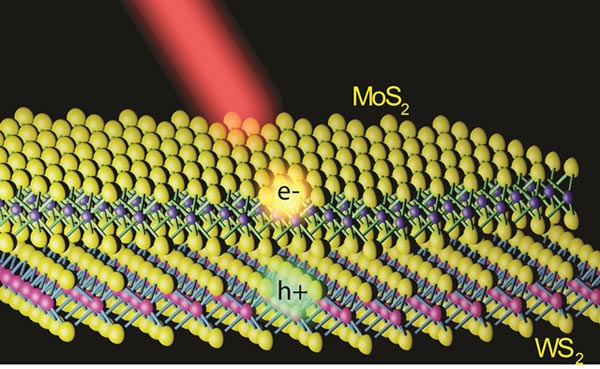
Illustration of a MoS2/WS2 heterostructure with a MoS2 monolayer lying on top of a WS2 monolayer. Electrons and holes created by light are shown to separate into different layers. (Image courtesy of Feng Wang group)
A new argument has just been added to the growing case for graphene being bumped off its pedestal as the next big thing in the high-tech world by the two-dimensional semiconductors known as MX2 materials.
An international collaboration of researchers led by a scientist with the U.S. Department of Energy (DOE)’s Lawrence Berkeley National Laboratory (Berkeley Lab) has reported the first experimental observation of ultrafast charge transfer in photo-excited MX2 materials.
The recorded charge transfer time clocked in at under 50 femtoseconds, comparable to the fastest times recorded for organic photovoltaics.
“We’ve demonstrated, for the first time, efficient charge transfer in MX2 heterostructures through combined photoluminescence mapping and transient absorption measurements,” says Feng Wang, a condensed matter physicist with Berkeley Lab’s Materials Sciences Division and the University of California (UC) Berkeley’s Physics Department.
“Having quantitatively determined charge transfer time to be less than 50 femtoseconds, our study suggests that MX2 heterostructures, with their remarkable electrical and optical properties and the rapid development of large-area synthesis, hold great promise for future photonic and optoelectronic applications.”
Wang is the corresponding author of a paper in Nature Nanotechnology describing this research. The paper is titled “Ultrafast charge transfer in atomically thin MoS2/WS2 heterostructures.” Co-authors are Xiaoping Hong, Jonghwan Kim, Su-Fei Shi, Yu Zhang, Chenhao Jin, Yinghui Sun, Sefaattin Tongay, Junqiao Wu and Yanfeng Zhang.
MX2 monolayers consist of a single layer of transition metal atoms, such as molybdenum (Mo) or tungsten (W), sandwiched between two layers of chalcogen atoms, such as sulfur (S). The resulting heterostructure is bound by the relatively weak intermolecular attraction known as the van der Waals force. These 2D semiconductors feature the same hexagonal “honeycombed” structure as graphene and superfast electrical conductance, but, unlike graphene, they have natural energy band-gaps. This facilitates their application in transistors and other electronic devices because, unlike graphene, their electrical conductance can be switched off.
“Combining different MX2 layers together allows one to control their physical properties,” says Wang, who is also an investigator with the Kavli Energy NanoSciences Institute (Kavli-ENSI). “For example, the combination of MoS2 and WS2 forms a type-II semiconductor that enables fast charge separation. The separation of photoexcited electrons and holes is essential for driving an electrical current in a photodetector or solar cell.”
In demonstrating the ultrafast charge separation capabilities of atomically thin samples of MoS2/WS2 heterostructures, Wang and his collaborators have opened up potentially rich new avenues, not only for photonics and optoelectronics, but also for photovoltaics.
“MX2 semiconductors have extremely strong optical absorption properties and compared with organic photovoltaic materials, have a crystalline structure and better electrical transport properties,” Wang says. “Factor in a femtosecond charge transfer rate and MX2 semiconductors provide an ideal way to spatially separate electrons and holes for electrical collection and utilization.”
Wang and his colleagues are studying the microscopic origins of charge transfer in MX2 heterostructures and the variation in charge transfer rates between different MX2 materials.
“We’re also interested in controlling the charge transfer process with external electrical fields as a means of utilizing MX2 heterostructures in photovoltaic devices,” Wang says.
This research was supported by an Early Career Research Award from the DOE Office of Science through UC Berkeley, and by funding agencies in China through the Peking University in Beijing.
Additional Information
For more about the research of Feng Wang go here
Lawrence Berkeley National Laboratory addresses the world’s most urgent scientific challenges by advancing sustainable energy, protecting human health, creating new materials, and revealing the origin and fate of the universe. Founded in 1931, Berkeley Lab’s scientific expertise has been recognized with 13 Nobel prizes. The University of California manages Berkeley Lab for the U.S. Department of Energy’s Office of Science. For more, visit www.lbl.gov.
The DOE Office of Science is the single largest supporter of basic research in the physical sciences in the United States and is working to address some of the most pressing challenges of our time. For more information, please visit science.energy.gov.
Media Contact
More Information:
http://newscenter.lbl.gov/2014/08/26/competition-for-graphene/All latest news from the category: Materials Sciences
Materials management deals with the research, development, manufacturing and processing of raw and industrial materials. Key aspects here are biological and medical issues, which play an increasingly important role in this field.
innovations-report offers in-depth articles related to the development and application of materials and the structure and properties of new materials.


Newest articles

Silicon Carbide Innovation Alliance to drive industrial-scale semiconductor work
Known for its ability to withstand extreme environments and high voltages, silicon carbide (SiC) is a semiconducting material made up of silicon and carbon atoms arranged into crystals that is…

New SPECT/CT technique shows impressive biomarker identification
…offers increased access for prostate cancer patients. A novel SPECT/CT acquisition method can accurately detect radiopharmaceutical biodistribution in a convenient manner for prostate cancer patients, opening the door for more…

How 3D printers can give robots a soft touch
Soft skin coverings and touch sensors have emerged as a promising feature for robots that are both safer and more intuitive for human interaction, but they are expensive and difficult…

