Miniaturized infrared detectors
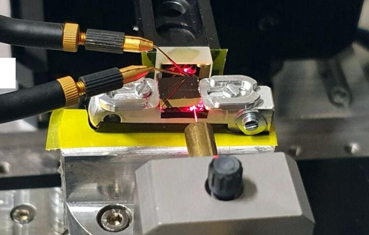
The experimental setup: A red alignment laser was used to visualize the beam path from the fiber into the optical waveguide and its reflection at a gold mirror. Two microprobes were used to contact the photoconductor, the size of which is in the subwavelength range. Image: Empa

Integration on a chip.

Extreme miniaturization of infrared (IR) detectors is critical for their integration into next-generation consumer electronics, wearables and ultra-small satellites. Thus far, however, IR detectors have relied on bulky (and expensive) materials and technologies. A team of scientists lead by Empa researcher Ivan Shorubalko now succeeded in developing a cost-effective miniaturization process for IR spectrometers based on a quantum dot photodetector, which can be integrated on a single chip, as they report in Nature Photonics.
Miniaturization of infrared spectrometers will lead to their wider use in consumer electronics, such as smartphones enabling food control, the detection of hazardous chemicals, air pollution monitoring and wearable electronics. They can be used for the quick and easy detection of certain chemicals without using laboratory equipment. Moreover, they can be useful for the detection of counterfeit medical drugs as well as of greenhouse gases such as methane and CO2.
A Team of scientists at Empa, ETH Zurich, EPFL, the University of Salamanca, Spain, the European Space Agency (ESA) and the University of Basel now built a proof-of-concept miniaturized Fourier-transform waveguide spectrometer that incorporates a subwavelength photodetector as a light sensor, consisting of colloidal mercury telluride quantum dot (Hg Te) and compatible with complementary metal-oxide-semiconductor (CMOS) technology, as they report in the recent issue of Nature Photonics.

/documents/56164/22738346/IR-QD_F-spectrometer-Grafik-web/261edf46-ddf0-4bcc-9433-92e392ba4ed1?t=1666626304400

This is how the IR spectrometer works: The photodetector, fabricated on top of a surface optical waveguide, consists of a bottom gold electrode at the bottom functioning as a scattering center, a photoactive layer (consisting of colloidal mercury telluride – HgTe – quantum dots), and a top gold electrode. By moving the mirror, the measured photocurrent maps the light intensity of the standing wave. i.e. the IR light. A Fourier transformation of the measured signal gives the optical spectra. Image: Lars Lüder
Tremendous effects on spectrometers of different kinds – and in various fields
The resulting spectrometer exhibits a large spectral bandwidth and moderate spectral resolution of 50 cm−1 at a total active spectrometer volume below 100 μm × 100 μm × 100 μm. This ultra-compact spectrometer design allows the integration of optical-analytical measurement instruments into consumer electronics and space devices. “The monolithic integration of subwavelength IR photodetectors has a tremendous effect on the scaling of Fourier-transform waveguide spectrometers”, says Empa researcher Ivan Shorubalko. “But this may also be of great interest for miniaturized Raman spectrometers, biosensors and lab-on-a-chip devices as well as the development of high-resolution snapshot hyperspectral cameras.”
Further information
Dr. Ivan Shorubalko
Transport at Nanoscale Interfaces
Phone +41 58 765 48 74
ivan.shorubalko@empa.ch
Editor / Media contact
Rainer Klose
Communications
Tel. +41 58 765 47 33
redaktion@empa.ch
Literature
MJ Grotevent, S Yakunin, D Bachmann, C Romero, JR. Vázquez de Aldana, M Madi, Michel Calame, MV Kovalenko, I Shorubalko; Integrated photodetectors for compact Fourier-transform waveguide spectrometers; Nature Photonics (2022); DOI: 10.1038/s41566-022-01088-7

Media Contact

Rainer Klose Communications
Empa - Eidgenössische Materialprüfungs- und Forschungsanstalt

All latest news from the category: Information Technology

Here you can find a summary of innovations in the fields of information and data processing and up-to-date developments on IT equipment and hardware.

This area covers topics such as IT services, IT architectures, IT management and telecommunications.

Back to home

Comments (0)

Write a comment

Newest articles

The last missing piece of silicon photonics

International research team presents first electrically pumped continuous-wave semiconductor laser suitable for seamless silicon integration. Scientists from Forschungszentrum Jülich, FZJ, the University of Stuttgart, and the Leibniz Institute for High…

Space-time crystals, an important step toward new optical materials

KIT scientists design tailored materials for optical information processing. Photonic space-time crystals are materials that could increase the performance and efficiency of wireless communication or laser technologies. They feature a…

Quasiparticle loss in extreme quantum materials

A new study by Rice University physicist Qimiao Si unravels the enigmatic behaviors of quantum critical metals — materials that defy conventional physics at low temperatures. Published in Nature Physics…