Low bandwidth? Use more colors at once
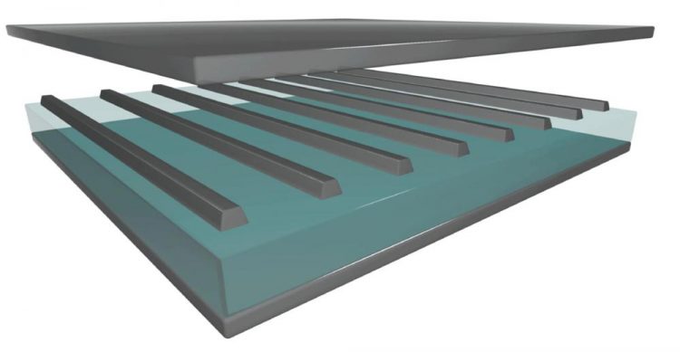
New ultrathin nanocavities with embedded silver strips have streamlined color production, and therefore broadened possible bandwidth, for both today's electronics and future photonics. Credit: Purdue University image/Alexander Kildishev
The rainbow is not just colors – each color of light has its own frequency. The more frequencies you have, the higher the bandwidth for transmitting information.
Only using one color of light at a time on an electronic chip currently limits technologies based on sensing changes in scattered color, such as detecting viruses in blood samples, or processing airplane images of vegetation when monitoring fields or forests.
Putting multiple colors into service at once would mean deploying multiple channels of information simultaneously, broadening the bandwidth of not only today's electronics, but also of the even faster upcoming “nanophotonics” that will rely on photons – fast and massless particles of light – rather than slow and heavy electrons to process information with nanoscale optical devices.
IBM and Intel have already developed supercomputer chips that combine the higher bandwidth of light with traditional electronic structures.
As researchers engineer solutions for eventually replacing electronics with photonics, a Purdue University-led team has simplified the manufacturing process that allows utilizing multiple colors at the same time on an electronic chip instead of a single color at a time.
The researchers also addressed another issue in the transition from electronics to nanophotonics: The lasers that produce light will need to be smaller to fit on the chip.
“A laser typically is a monochromatic device, so it's a challenge to make a laser tunable or polychromatic,” said Alexander Kildishev, associate professor of electrical and computer engineering at Purdue University. “Moreover, it's a huge challenge to make an array of nanolasers produce several colors simultaneously on a chip.”
This requires downsizing the “optical cavity,” which is a major component of lasers. For the first time, researchers from Purdue, Stanford University and the University of Maryland embedded so-called silver “metasurfaces” – artificial materials thinner than light waves – in nanocavities, making lasers ultrathin.
“Optical cavities trap light in a laser between two mirrors. As photons bounce between the mirrors, the amount of light increases to make laser beams possible,” Kildishev said. “Our nanocavities would make on-a-chip lasers ultrathin and multicolor.”
Currently, a different thickness of an optical cavity is required for each color. By embedding a silver metasurface in the nanocavity, the researchers achieved a uniform thickness for producing all desired colors. Their findings appear in Nature Communications.
“Instead of adjusting the optical cavity thickness for every single color, we adjust the widths of metasurface elements,” Kildishev said.
Optical metasurfaces could also ultimately replace or complement traditional lenses in electronic devices.
“What defines the thickness of any cell phone is actually a complex and rather thick stack of lenses,” Kildishev said. “If we can just use a thin optical metasurface to focus light and produce images, then we wouldn't need these lenses, or we could use a thinner stack.”
###
A patent has been filed for this technology. The work was supported by the Air Force Office of Scientific Research (AFOSR) MURI grant FA9550-14-1-0389 and the Defense Advanced Research Projects Agency's Defense Sciences Office Extreme Optics and Imaging (EXTREME) program, Award HR00111720032.
ABSTRACT
Ultrathin and multicolor optical cavities with embedded metasurfaces
Amr M. Shaltout1,2, Jongbum Kim1,3, Alexandra Boltasseva1, Vladimir M. Shalaev1& Alexander V. Kildishev1
1Purdue University, West Lafayette, IN, USA
2Stanford University, Stanford, CA, USA
3University of Maryland, College Park, MD, USA
doi: 10.1038/s41467-018-05034-6
Over the past years, photonic metasurfaces have demonstrated their remarkable and diverse capabilities in advanced control over light propagation. Here, we demonstrate that these artificial films of deeply subwavelength thickness also offer new unparalleled capabilities in decreasing the overall dimensions of integrated optical systems. We propose an original approach of embedding a metasurface inside an optical cavity–one of the most fundamental optical elements–to drastically scale-down its thickness. By modifying the Fabry-Pérot interferometric principle, this methodology is shown to reduce the metasurface-based nanocavity thickness below the conventional λ/(2n) minimum. In addition, the nanocavities with embedded metasurfaces can support independently tunable resonances at multiple bands. As a proof-of-concept, using nanostructured metasurfaces within 100-nm nanocavities, we experimentally demonstrate high spatial resolution color filtering and spectral imaging. The proposed approach can be extrapolated to compact integrated optical systems on-a-chip such as VCSEL's, high-resolution spatial light modulators, imaging spectroscopy systems, and bio-sensors.
Media Contact
All latest news from the category: Information Technology
Here you can find a summary of innovations in the fields of information and data processing and up-to-date developments on IT equipment and hardware.
This area covers topics such as IT services, IT architectures, IT management and telecommunications.


Newest articles

Properties of new materials for microchips
… can now be measured well. Reseachers of Delft University of Technology demonstrated measuring performance properties of ultrathin silicon membranes. Making ever smaller and more powerful chips requires new ultrathin…

Floating solar’s potential
… to support sustainable development by addressing climate, water, and energy goals holistically. A new study published this week in Nature Energy raises the potential for floating solar photovoltaics (FPV)…

Skyrmions move at record speeds
… a step towards the computing of the future. An international research team led by scientists from the CNRS1 has discovered that the magnetic nanobubbles2 known as skyrmions can be…

