Laser-manufactured customized lenses
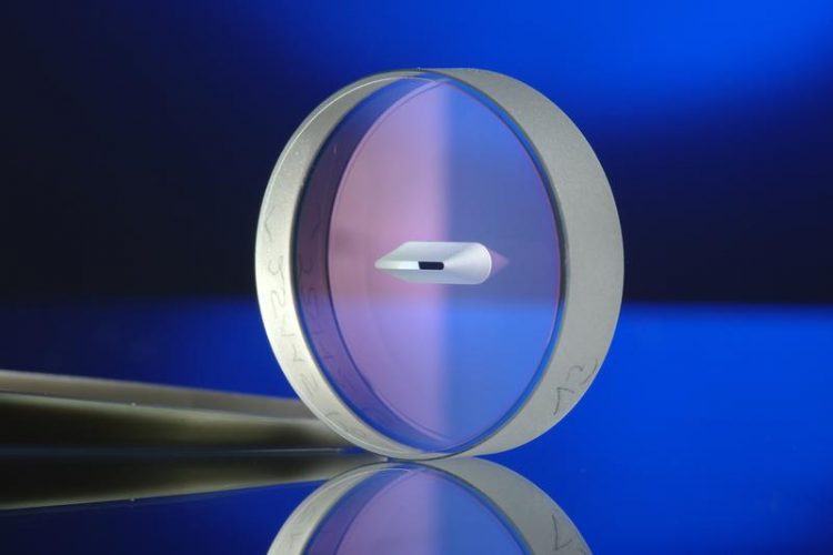
Fused silica with a slit, made by processing with inverse laser drilling; thickness: 6.35 mm, angle of the undercut: approx. 10°. Fraunhofer ILT, Aachen, Germany.
Scientists at Fraunhofer ILT in Aachen are researching new laser processes for shaping, polishing, structuring and assembling optics and components made of various optical glasses and fused silica.
One focus is on developing a completely laser-based digital process chain for producing aspheres and free-form optics. At the international trade fair for optical technologies, components and systems, scientists are presenting project results and demonstrators from the various areas of research.
Laser-based process chain for the production of free-form optics
To shape the form of the optics the glass is removed in layers with an ablation rate of up to several mm³/s. A subsequent laser polishing process smooths the surface by remelting a thin surface layer without removing material – at surface rates of up to 5 cm2/s. The result is a roughness extending into the subnanometer range. Through a final thin-layer removal, called laser beam figuring, layer thicknesses in the nanometer range can again be locally removed through an evaporation process (to ablation depths below 5 nm, with a lateral spatial resolution of less than 100 µm). This step is being developed to reduce any remaining long-wave roughnesses and form errors that cannot be removed during laser polishing.
Design of free-form optics
The freeformOPT software developed in Aachen allows various free-form optical surfaces to be calculated with over 100,000 degrees of freedom and also provides interfaces to CAD and optical software. The CAD drawings can be directly used on the appropriate production machines.
Geometrical freedom and economic efficiency through the use of lasers
In contrast to conventional grinding and polishing processes, processes in contactless laser processing are largely wear-free. Low spot diameters and controllable intensity profiles permit a high degree of geometrical freedom for surfaces. Process cycle times are short and almost independent of the complexity of the surface, be it sphere, asphere or free-form optic.
Possible areas of application for optical elements produced in this way can be found, for instance, in interior and exterior lighting, car manufacturing or laser optics. By structuring the reverse side of optical components, the weight of components can be reduced for, say, lightweight designs.
Wide variety of laser material processing at Optatec 2016
With inverse laser drilling, holes are drilled into dielectric materials with high aspect ratios (~1:200). One application for this process is drilling holes that measure 100 µm in mirror substrates without causing conchoidal fractures. This is used to overlap or separate beams, but also to structure photonic fiber preforms with a high degree of geometrical freedom.
Robust optomechanical components that will be applied in pulsed lasers for satellite-based climate research will also be on display. Special tilt stabilities of individual key components are achieved through solder joints. In addition, foregoing the use of organic substances achieves low outgassing rates and thus long service lives.
With glass frit bonding, the spatially restricted injection of laser light into the joint area is used to obtain homogenous and crack-free joints, making it possible to encapsulate sensitive OLED layers or microsensors. Various applications of the process up to a size of 340 mm x 340 mm are shown as examples.
Our experts at Optatec 2016
At the international trade fair in Frankfurt, Fraunhofer ILT will be at the joint Fraunhofer booth (Hall 3.0, D50) to present current research results. Around 570 exhibitors will also be at the trade fair to display innovations and new developments in the areas of optical technologies, components and systems.
Contact
Dipl.-Phys., Dipl.-Volksw. Dominik Esser
Group Solid State Lasers
Phone +49 241 8906-437
dominik.esser@ilt.fraunhofer.de
Dr.-Ing. Edgar Willenborg
Group Manager Polishing
Phone +49 241 8906-213
edgar.willenborg@ilt.fraunhofer.de
Fraunhofer Institute for Laser Technology ILT
Steinbachstraße 15
52074 Aachen, Germany
Media Contact
All latest news from the category: Trade Fair News


Newest articles
Combatting disruptive ‘noise’ in quantum communication
In a significant milestone for quantum communication technology, an experiment has demonstrated how networks can be leveraged to combat disruptive ‘noise’ in quantum communications. The international effort led by researchers…
Stretchable quantum dot display
Intrinsically stretchable quantum dot-based light-emitting diodes achieved record-breaking performance. A team of South Korean scientists led by Professor KIM Dae-Hyeong of the Center for Nanoparticle Research within the Institute for…
Internet can achieve quantum speed with light saved as sound
Researchers at the University of Copenhagen’s Niels Bohr Institute have developed a new way to create quantum memory: A small drum can store data sent with light in its sonic…

