Galliumnitrit-Halbleiter
The invention relates to a method to wax of gallium nitride
semiconductor material on a sapphire substrate. The substrate can serve for the production of electronic components or as substrate for the epitaxy of other layers. The method of the invention is easy to realize and suited for the industrial application. It further assures the production of highquality GaN layers.
Further Information: PDF
PVA Mecklenburg-Vorpommern AG
Phone: +49 (0)381/49 74 74 0
Contact
Moritz v. Grotthuss, Dr. Rüdiger Werp
Media Contact
All latest news from the category: Technology Offerings
Newest articles
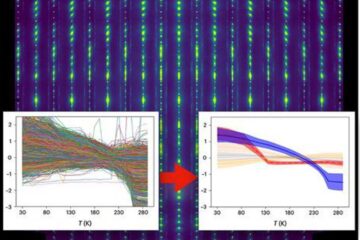
Machine learning algorithm reveals long-theorized glass phase in crystal
Scientists have found evidence of an elusive, glassy phase of matter that emerges when a crystal’s perfect internal pattern is disrupted. X-ray technology and machine learning converge to shed light…
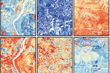
Mapping plant functional diversity from space
HKU ecologists revolutionize ecosystem monitoring with novel field-satellite integration. An international team of researchers, led by Professor Jin WU from the School of Biological Sciences at The University of Hong…
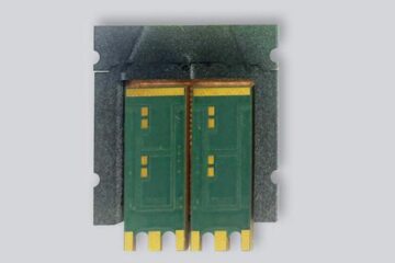
Inverters with constant full load capability
…enable an increase in the performance of electric drives. Overheating components significantly limit the performance of drivetrains in electric vehicles. Inverters in particular are subject to a high thermal load,…

