Start of the "CIS Cluster Tool" project on the research of a new manufacturing process …
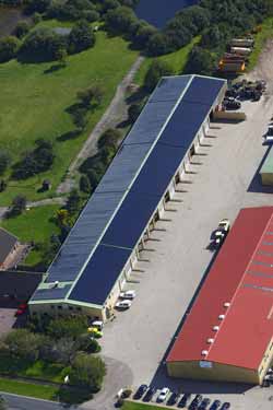
CIS-Photovoltaic plant with AVANCIS PowerMax® Modules. © AVANCIS<br>
The “CIS Cluster Tool” project is starting its work on the development of new manufacturing procedures for copper indium selenide-based thin film semiconductors (CIS) as part of a sponsoring project within the “Photovoltaics Innovations Alliance”. The research project is being carried out in cooperation of leading German companies in the photovoltaic industry. The project is to make a significant contribution to securing the global competitiveness of the German photovoltaics and supply industry in the medium and long term.
The substantial and sustainable expansion of renewable energies is one of the central tasks of our time. The direct conversion of sunlight into electricity (photovoltaics) represents high quality technology that is of particular interest amongst all possible procedures. In order to secure the leading role played by Germany in the high-tech photovoltaic sector, the Federal Ministry of Education and Research (BMBF) and the Federal Ministry of the Environment, Nature Conservation and Nuclear Safety (BMU) announced the “Photovoltaic Innovations Alliance” sponsorship programme last year. From just under 120 applications received, the CIS Cluster Tool joint project, which is dedicated to researching a new manufacturing process for CIS semiconductor panels, was chosen amongst others as particularly promising. CIS technology, which is based on semiconductor film made from copper (Cu), Indium (In) and Selenide (Se) as well as Gallium (Ga), is one of the most promising photovoltaic technologies and offers significant future potential.
CIS Cluster Tool: New plant concepts, new full process chains and new analytics.
The overall project objective of the working group is to research a new manufacturing process for CIS semiconductor films in order to achieve the highest level of efficiency of thin film solar modules combined with a significant increase of plant throughput compared with existing concepts. An industrial manufacturing process is to be developed on the basis of findings from a planned demonstration plant, with which the costs of manufacturing thin film photovoltaic modules per watt peak can be significantly reduced.
In order to achieve the overall project objective, the following significant development themes are being pursued:
• New plant concepts and processes: Research of innovative RTP (Rapid Thermal Processing) plant concepts and processes which can be implemented on an industrial scale and are in-line capable, in order to achieve the highest level of efficiency in short cycle times.
• New full process chains: Combination of selenide coating with the following RTP of CIS semiconductors in order to achieve increased process control, higher efficiency combined with improved plant technology in order to reduce manufacturing costs.
• New in-situ analytics: Research of new in-situ measurement processes in order to improve process control and the understanding of physicochemical processes in semiconductor production. Use of knowledge on process optimisation with regard to optimising efficiency and minimising processing time.
The CIS Cluster Tool joint project is a cooperation between four experienced partners from different levels of the value chain in the photovoltaics industry: AVANCIS GmbH & Co. KG, (manufacturer of CIS photovoltaic modules), SINGULUS TECHNOLOGIES AG (plant construction), HERAEUS Noblelight GmbH (infrared heating technology) and the IfG Institute for Scientific Instruments GmbH (innovative measurement techniques). As a result of the collaboration between the four leading German companies, synergy effects are expected in order to achieve the demanding project objectives. The project is invested for three years and is financed by funds from the “Photovoltaic Innovations Alliance” funding initiative amounting to 2.9 m euros and by contributions of the participating companies.
Any further questions on the work of the “CIS Cluster Tool” joint project can be answered by:
Dr Franz Karg, CTO
AVANCIS GmbH & Co. KG
Otto-Hahn-Ring 6, 81739 Munich, Germany
Phone +49 (0)89 219620-500
Mobile: +49 (0)171 3043200
Fax: +49 (0)89 219620-501
Franz.Karg@avancis.de
www.avancis.de
More information on the “CIS Cluster Tool” joint project partners:
About AVANCIS GmbH & Co. KG:
AVANCIS develops and manufactures photovoltaic modules based on CIS (Copper Indium Selenide) and is a part of the global Saint-Gobain Group. The innovative manufacturing process relies on the second-generation CIS technology developed by the AVANCIS research & development department in Munich. The first plant at the company’s headquarters in Torgau has a production capacity of 20 megawatt peak per year (MWp/a). The company is currently building a second plant in Torgau with an annual capacity of 100 MWp and is building a third plant of 100 MWp/a in South Korea as part of the production joint venture “Hyundai-AVANCIS”.
About SINGULUS TECHNOLOGIES AG:
With the innovative vacuum coating systems, wet chemical in-line cell cleaning and etching systems as well as patented new procedures for the manufacture of thin film solar cells, SINGULUS is advancing its expansion in the solar market. SINGULUS is intensively expanding activities in the solar and optical disc segments. The objective is to hold a leading position in silicon and thin film solar technology and to maintain its technological leadership in the solar and optical disc markets.
For further information, please contact:
Bernhard Krause, company spokesman
SINGULUS TECHNOLOGIES AG
Hanauer Landstraße 103,
D-63796 Kahl/Main, ISIN: DE0007238909, WKN: 723890
Phone + 49 (0) 6181 982 80 20
Bernhard.krause@singulus.de
www.singulus.de
About HERAEUS Noblelight GmbH:
Heraeus Noblelight GmbH counts itself among the market and technology leaders worldwide for the manufacture of specialist light sources. In 2009, Heraeus Noblelight generated annual sales of €71.6 million and had 707 employees worldwide. The Industrial Process Technology Division in Kleinostheim develops, produces and sells infrared emitters and systems for modern heating process in industrial production. Since the 50's, Heraeus infrared heating technology has been successful in the automobile industry, drying of lacquer and colour, processing plastics, glass or textiles as well as the manufacture of solar cells or innovative materials.
For further information, please contact:
Dr Sven Linow
Heraeus Noblelight GmbH
Development Industrial Process Technology
Reinhard-Heraeus-Ring 7
63801 Kleinostheim
Germany
Phone +49 (0) 6181 35-4856
Fax +49 (0) 6181 35-16 4856
Sven.linow@heraeus.com
www.heraeus-noblelight.com/infrared
About the IfG Institute for Scientific Instruments GmbH:
The IfG Institute for Scientific Instruments GmbH is a medium-sized enterprise, whose core competence is the development and industrial production of micro and nano-structured glass as high precision capillary optics for beam shaping of x-rays which is a unique selling point in Europe. Its strengths also include the development and manufacturing of devices and components for x-ray analysis, especially process-oriented in- and off-line metrology. The company's range of products includes single components such as the modular x-ray source iMOXS and complex industrial devices such as the XRF scanner ELBRUS iXSCAN for continuous in-line use.
For further information, please contact:
Dr Aniouar Bjeoumikhov, CEO
IfG Institute for Scientific Instruments GmbH
Rudower Chaussee 29/ 31, 12489 Berlin, Germany
phone +49 (0)30 63 92 65 00
fax: +49 (0)30 63 92 65 01
Bjeoumikhov@ifg-adlershof.de
www.ifg-adlershof.de
Media Contact
More Information:
http://www.heraeus-noblelight.comAll latest news from the category: Process Engineering
This special field revolves around processes for modifying material properties (milling, cooling), composition (filtration, distillation) and type (oxidation, hydration).
Valuable information is available on a broad range of technologies including material separation, laser processes, measuring techniques and robot engineering in addition to testing methods and coating and materials analysis processes.


Newest articles

Properties of new materials for microchips
… can now be measured well. Reseachers of Delft University of Technology demonstrated measuring performance properties of ultrathin silicon membranes. Making ever smaller and more powerful chips requires new ultrathin…

Floating solar’s potential
… to support sustainable development by addressing climate, water, and energy goals holistically. A new study published this week in Nature Energy raises the potential for floating solar photovoltaics (FPV)…

Skyrmions move at record speeds
… a step towards the computing of the future. An international research team led by scientists from the CNRS1 has discovered that the magnetic nanobubbles2 known as skyrmions can be…

