New technique producing small things in large quantities

Although relatively new to the market, liquid crystal display (LCD) televisions soon may be obsolete, thanks to a new technique created by University of Houston professors.
Vincent Donnelly, Demetre Economou and Paul Ruchhoeft, all of the Cullen College of Engineering, have developed a technique that allows nanotech devices to be mass-produced, which could move the television industry away from the LCD display to the superior field emission display (FED). FEDs use a large array of carbon nanotubes – the most efficient emitters known – to create a higher resolution picture than an LCD.
The nanotech fabrication technique that can mass produce an ordered array of carbon nanotubes and make FEDs happen promises to remove some of the largest practical barriers to mass-producing nanotech devices, Economou said.
Dubbed nanopantography, the method uses standard photolithography to selectively remove parts of a thin film and etching to create arrays of ion-focusing micro-lenses – small round holes through a metal structure – on a substrate, such as a silicon wafer.
“These lenses act as focusing elements,” Donnelly said. “They focus the beamlets to fabricate a hole 100 times smaller than the lens size.”
A beam of ions is then directed at the substrate. When the wafer is tilted, the desired pattern is replicated simultaneously in billions of many closely spaced holes over an area, limited only by the size of the ion beam.
“The nanostructures that you can form out of that focusing can be written simultaneously over the whole wafer in predetermined positions,” Economou said. “Without our technique, nanotech devices can be made with electron-beam writing or with a scanning tunneling microscope. However, the throughput, or fabrication speed, is extremely slow and is not suitable for mass production or for producing nanostructures of any desired shape and material.”
With the right ions and gaseous elements, the nanotech fabrication method can be used to etch a variety of materials and virtually any shape with nanosize dimensions. A standard printing technique that can create lenses measuring 100 nanometers wide could be used to draw features just one nanometer wide if combined with nanopantography.
“We expect nanopantography to become a viable method for rapid, large-scale fabrication,” Donnelly said. Economou, Donnelly and Ruchhoeft have been working on the technology for four years. UH filed the patent application in December 2006. They hope the technology can become commercially available in five to 10 years and expect it to become a viable method for large-scale production.
About the University of Houston
The University of Houston, Texas’ premier metropolitan research and teaching institution, is home to more than 40 research centers and institutes and sponsors more than 300 partnerships with corporate, civic and governmental entities. UH, the most diverse research university in the country, stands at the forefront of education, research and service with more than 35,000 students.
About the Cullen College of Engineering
UH Cullen College of Engineering has produced five U.S. astronauts, ten members of the National Academy of Engineering, and degree programs that have ranked in the top ten nationally. With more than 2,600 students, the college offers accredited undergraduate and graduate degrees in biomedical, chemical, civil and environmental, electrical and computer, industrial, and mechanical engineering. It also offers specialized programs in aerospace, materials, petroleum engineering and telecommunications.
Media Contact
More Information:
http://www.uh.eduAll latest news from the category: Process Engineering
This special field revolves around processes for modifying material properties (milling, cooling), composition (filtration, distillation) and type (oxidation, hydration).
Valuable information is available on a broad range of technologies including material separation, laser processes, measuring techniques and robot engineering in addition to testing methods and coating and materials analysis processes.
Newest articles

Properties of new materials for microchips
… can now be measured well. Reseachers of Delft University of Technology demonstrated measuring performance properties of ultrathin silicon membranes. Making ever smaller and more powerful chips requires new ultrathin…

Floating solar’s potential
… to support sustainable development by addressing climate, water, and energy goals holistically. A new study published this week in Nature Energy raises the potential for floating solar photovoltaics (FPV)…
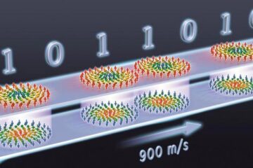
Skyrmions move at record speeds
… a step towards the computing of the future. An international research team led by scientists from the CNRS1 has discovered that the magnetic nanobubbles2 known as skyrmions can be…


