Laser Instead Of A Diamond Saw
St. Petersburg physicists have developed a plant that allows to cut sapphire crystals into almost ideally smooth plates being fractions of millimeter thick. The approach suggested by the researchers fundamentally differs from the traditional one. They suggest that sapphire should not be sawn by a saw, but split by laser.
It is quite common that a title like “A plant for laser scribing of sapphire wafers” would surprise an ordinary person but it sounds like music for specialists. It is an exceptionally useful, and unique device produced in St. Petersburg by the specialists of the MULTITECH company. It is intended to produce multiple individual finished microchips out of a whole sapphire plate with marked chip structures called “wafers”.
Microchips on sapphire and quartz substrates have been made so far in a simple and rough way: the crystal is slit by a thin metal disk with diamantine. The process is extremely unproductive. On the one hand, the disc possesses its own thickness that makes hundreds of microns. On the other hand, due to such rough processing the edges of the slit plates are covered by cracks all over. That is why a major part of the material is wasted – only one third or a quarter of feedstock can be used for the above purpose.
The device designed by the specialists of the MILTITECH company is based on fundamentally different principles. The device does not saw a crystal but incises or scribes it by laser. Speaking to the point, the device using a special laser produces deep and straight cracks in the crystal in previously selected spots and in preset direction. These cracks allow to easily and simply break the sapphire plate “cracked” by laser into multiple tiny microchips – for example, into small square of 1 mm x 1 mm in dimension. This is done by a small and also original instrument resembling a diminutive photograph cutter.
Peculiarity of the device is that instead of a powerful laser it is suggested to use a low energy laser but with a supershort pulse time, the so-called a picosecond one. An original optical system is also used allowing to focus the laser beam into a very thin sheaf being only several microns in diameter. As a result, the beam’s energy concentrates in space and time and splits the crystal from inside without evaporating it. The device is shooting by short laser bursts – i.e., series of picosecond impulses. That is how point defects are formed resembling a perforation line. It is along these lines that the crystal splits, i.e. a deep crack goes from one defect to another, joining them.
Firstly, these transverse cracks are small and much less numerous than those formed while cutting the crystal by a diamond disc, and secondly, the cracks partly “overgrow” by themselves. The researchers made sure of that due to a microscopical television system also designed by them. Under computer control, the “cutting” is performed quickly and automatically. But there is one more valuable advantage. As the beam can be focused with extreme precision, the crystal can be cut when it is in the plastic packing. The packing will not be damaged by the laser beam as it is not focused on packing. This peculiarity is difficult to overestimate. It gives the opportunity to process chips not in the specially equipped facilities with filtered air –the so-called clean rooms, but in ordinary ones.
Media Contact
More Information:
http://www.informnauka.ruAll latest news from the category: Process Engineering
This special field revolves around processes for modifying material properties (milling, cooling), composition (filtration, distillation) and type (oxidation, hydration).
Valuable information is available on a broad range of technologies including material separation, laser processes, measuring techniques and robot engineering in addition to testing methods and coating and materials analysis processes.


Newest articles
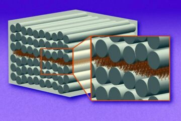
“Nanostitches” enable lighter and tougher composite materials
In research that may lead to next-generation airplanes and spacecraft, MIT engineers used carbon nanotubes to prevent cracking in multilayered composites. To save on fuel and reduce aircraft emissions, engineers…
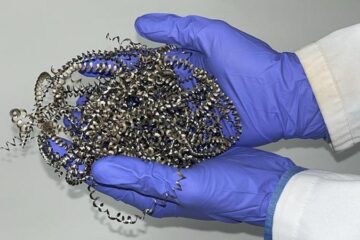
Trash to treasure
Researchers turn metal waste into catalyst for hydrogen. Scientists have found a way to transform metal waste into a highly efficient catalyst to make hydrogen from water, a discovery that…
Real-time detection of infectious disease viruses
… by searching for molecular fingerprinting. A research team consisting of Professor Kyoung-Duck Park and Taeyoung Moon and Huitae Joo, PhD candidates, from the Department of Physics at Pohang University…

