High Speed Laser Soldering for Flexible Interconnection of Self-Bonding Copper Wires
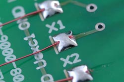
Demonstrator component to solder self-bonding wires on circuit boards. Source: Fraunhofer ILT
Manufacturing highly integrated, electro-engineering components in Europe primarily demands, in addition to high quality, a high amount of flexibility to remain competitive against the cost advantages found in low-wage countries. Manufacturing facilities have to be transferable to a wide variety of products, preferably without retooling.
In addition, quick, highly automated manufacturing procedures are necessary for largely unmanned manufacturing. Exposed to these requirements are small and medium-sized enterprises who occupy market segments for highly integrated electrical engineering components in small and medium quantities; such segments cannot be served by mass production facilities. Examples are innovative products from medical or sensor technology for which a significant production step is the interconnection of enamel-insulated coil wires to connection pads on a circuit board.
Currently, the interconnection is soldered manually for these products due to a lack of automation facilities. Since the process and the geometry of the component are complicated, the manufacturing process can only be reproduced with difficulty. The quality of the solder connection, thus, strongly depends upon the person conducting it. So that the insulating enamel layer is removed from the wire, the hot soldering iron has to be guided over the individual wire several times with a certain contact pressure – this way the insulating enamel melts and the bare wire surface contacts the liquid solder immediately. This method is not only time consuming, but also harbors a danger: the section of wire to be connected can tear when very thin self-bonding wires, e.g.
To increase the process speed and reproducibility, the Fraunhofer ILT has developed an automated laser soldering process that not only enhances the manufacturing flexibility, but also offers great potential for further miniaturization. With this process, the enamel removal and the interconnection take place in one single process step. On the one hand, the reproducibility is significantly increased via integrated process monitoring and control based on pyrometric sensors used in the laser-beam soldering process. On the other, the contactless laser soldering process offers significant potential for miniaturization in comparison to competing processes, since the dimensions of the connecting pads can be reduced down to several hundred micrometers.
This automated soldering process allows not only a nearly free choice of connection geometries, but also makes manufacturing so flexible that any number of quantities – even individual parts – can be produced without increasing reaction time, as a particular product requires. Medium-sized companies in the sector of electronic manufacturing can clearly fall back on the expertise of the Fraunhofer ILT.
Contact Partners at Fraunhofer ILT
Our experts would be glad to answer any questions you may have:
Dipl.-Ing. Felix Schmitt
Department of Microtechnology
Telephone +49 241 8906-322
felix.schmitt@ilt.fraunhofer.de
Dr. Arnold Gillner
Head, Department of Microtechnology
Telephone +49 241 8906-148
arnold.gillner@ilt.fraunhofer.de
Fraunhofer Institute for Laser Technology ILT
Steinbachstraße 15
52074 Aachen
Germany
Tel. +49 241 8906-0
Fax. +49 241 8906-121
Media Contact
All latest news from the category: Process Engineering
This special field revolves around processes for modifying material properties (milling, cooling), composition (filtration, distillation) and type (oxidation, hydration).
Valuable information is available on a broad range of technologies including material separation, laser processes, measuring techniques and robot engineering in addition to testing methods and coating and materials analysis processes.


Newest articles

Silicon Carbide Innovation Alliance to drive industrial-scale semiconductor work
Known for its ability to withstand extreme environments and high voltages, silicon carbide (SiC) is a semiconducting material made up of silicon and carbon atoms arranged into crystals that is…

New SPECT/CT technique shows impressive biomarker identification
…offers increased access for prostate cancer patients. A novel SPECT/CT acquisition method can accurately detect radiopharmaceutical biodistribution in a convenient manner for prostate cancer patients, opening the door for more…

How 3D printers can give robots a soft touch
Soft skin coverings and touch sensors have emerged as a promising feature for robots that are both safer and more intuitive for human interaction, but they are expensive and difficult…

