Cladding gold contacts with a laser
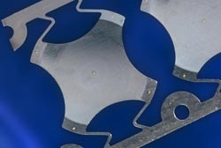
Gold contact spots on a snap dome.<br>Source: INOVAN<br>
Electroplating is the conventional method used for this purpose, but scientists have now developed a novel laser-based method which involves laser cladding gold contact spots instead of applying the gold in a thin layer on the whole surface. This new technique is fast and offers the potential to cut up to 90 percent of the amount of gold used.
Keys and keyboards have become a common sight in today’s world, both in our personal lives (cars, phones, computers) and in industrial settings. Users expect keys to operate with 100 percent reliability regardless of how many times they are pressed. At the same time, manufacturers are seeking cheaper production methods and new ways of making more efficient use of expensive, high-quality materials.
The Fraunhofer Institute for Laser Technology ILT in Aachen has developed a method of producing keys on an industrial scale which fulfills both these requirements. Within the scope of the Mifulas 2 project funded by Germany’s Federal Ministry of Education and Research (BMBF), researchers at Fraunhofer ILT – working in collaboration with their project partner INOVAN – have been drawing on their experience in laser cladding to replace the electroplated gold layers on switch contacts known as ‘snap domes’ with small welded gold spots.
Snap domes comprise small contact springs which are used to make electrical contact and provide tactile feedback in a wide range of keyboard designs. They generally consist of high-quality spring steel which is typically gold-plated or modified in some other way in order to achieve better contact and more reliable switching. As well as having low contact resistance, gold also boasts outstanding resistance to corrosion.
The new method replaces the conventional large gold surfaces with small contact spots which are cladded by a fiber laser. Using gold powder with grain diameters smaller than 10 µm, the fiber laser takes advantage of its beam diameter of less than 100 µm to create contact spots with a diameter and height of less than 100 µm. This micro laser cladding uses a nozzle to feed the gold powder into the interaction zone of the laser beam and the substrate material (e.g. stainless steel, nickel alloy). The laser energy melts both the gold powder and a thin surface layer of the substrate to create a welded spot which is metallurgical bonded to the substrate.
Significant reduction in material consumption
One of the biggest advantages of this new method is its material efficiency. To replace the thin gold layer deposited on snap domes by conventional methods, you need just five selectively welded gold contact spots – and initial calculations suggest that this slashes the amount of material required to make the gold contact by between 50 and 90 percent. Preliminary tests carried out by INOVAN comprising 100,000 switching operations demonstrate that this new approach does not measurably affect switch service life. In addition, the electrical properties of the gold contact spots correspond to the results obtained from electroplating.
Integrated production
The laser-based method also makes it possible to integrate the fabrication of the gold contact spots into the production of the switch components themselves. This enables rolls of material to be processed and facilitates the efficient production of short run batches and prototypes. Cladding a single point takes approximately 50 milliseconds. Researchers are currently investigating how to accelerate the process; experts consider that it should be possible to weld 20 contact spots simultaneously in the future by splitting the laser beam.
Using laser cladding to produce contacts from precious metals is a method that, in principle, is suitable for all metal parts which currently rely on plating techniques to make electrical contacts. Examples include the switches used in cell phones as well as bipolar plates for fuel cells.
Your contacts at Fraunhofer ILT
Our experts are on hand to answer your questions:
Dipl.-Phys. Matthias Belting
Coatings and Heat Treatment Group
Phone +49 241 8906-624
matthias.belting@ilt.fraunhofer.de
Dr. Andreas Weisheit
Head of Coatings and Heat Treatment Group
Phone +49 241 8906-403
andreas.weisheit@ilt.fraunhofer.de
Fraunhofer Institute for Laser Technology ILT
Steinbachstrasse 15
52074 Aachen
Phone +49 241 8906-0
Fax +49 241 8906-121
Media Contact
More Information:
http://www.ilt.fraunhofer.deAll latest news from the category: Process Engineering
This special field revolves around processes for modifying material properties (milling, cooling), composition (filtration, distillation) and type (oxidation, hydration).
Valuable information is available on a broad range of technologies including material separation, laser processes, measuring techniques and robot engineering in addition to testing methods and coating and materials analysis processes.


Newest articles
Bringing bio-inspired robots to life
Nebraska researcher Eric Markvicka gets NSF CAREER Award to pursue manufacture of novel materials for soft robotics and stretchable electronics. Engineers are increasingly eager to develop robots that mimic the…

Bella moths use poison to attract mates
Scientists are closer to finding out how. Pyrrolizidine alkaloids are as bitter and toxic as they are hard to pronounce. They’re produced by several different types of plants and are…
AI tool creates ‘synthetic’ images of cells
…for enhanced microscopy analysis. Observing individual cells through microscopes can reveal a range of important cell biological phenomena that frequently play a role in human diseases, but the process of…

