Stanford writes in world's smallest letters
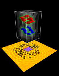
This is an electron wave quantum hologram displaying the initials \"SU\" of Stanford University. The yellow area is a copper surface. The holes in the copper are molecules of carbon monoxide. Constantly moving electrons on the surface of the copper bounce off the carbon monoxide molecules in predictable ways. With their dual wave/particle properties, the electron waves in the purple area create inference patterns that can store readable information, in this case, SU. To store information, the researchers arrange the molecule in specific patterns with a scanning tunneling microscope.<br>Credit: Stanford University<br>
Stanford researchers have reclaimed bragging rights for creating the world's smallest writing, a distinction the university first gained in 1985 and lost in 1990.
How small is the writing? The letters in the words are assembled from subatomic sized bits as small as 0.3 nanometers, or roughly one third of a billionth of a meter.
The researchers encoded the letters “S” and “U” (as in Stanford University) within the interference patterns formed by quantum electron waves on the surface of a sliver of copper. The wave patterns even project a tiny hologram of the data, which can be viewed with a powerful microscope.
“We miniaturized their size so drastically that we ended up with the smallest writing in history,” said Hari Manoharan, the assistant professor of physics who directed the work of physics graduate student Chris Moon and other researchers.
The quest for small writing has played a role in the development of nanotechnology for 50 years, beginning decades before “nano” became a household word. During a now-legendary talk in 1959, the remarkable physicist Richard Feynman argued that there were no physical barriers preventing machines and circuitry from being shrunk drastically. He called his talk “There's Plenty of Room at the Bottom.”
Feynman offered a $1,000 prize for anyone who could find a way to rewrite a page from an ordinary book in text 25,000 times smaller than the usual size (a scale at which the entire contents of the Encyclopedia Britannica would fit on the head of a pin). He held onto his money until 1985, when he mailed a check to Stanford grad student Tom Newman, who, working with electrical engineering Professor Fabian Pease, used electron beam lithography to engrave the opening page of Dickens' A Tale of Two Cities in such small print that it could be read only with an electron microscope.
That record held until 1990, when researchers at a certain computer company famously spelled out the letters IBM by arranging 35 individual xenon atoms.
Now, in a paper published online in the journal Nature Nanotechnology, the Stanford researchers describe how they have created letters 40 times smaller than the original prize-winning effort and more than four times smaller than the IBM initials. (http://www.youtube.com/watch?v=j3QQJEHuefQ)
Working in a vibration-proof basement lab in the Varian Physics Building, Manoharan and Moon began their writing project with a scanning tunneling microscope, a device that not only sees objects at a very small scale but also can be used to move around individual atoms. The Stanford team used it to drag single carbon monoxide molecules into a desired pattern on a copper chip the size of a fingernail.
On the two-dimensional surface of the copper, electrons zip around, behaving as both particles and waves, bouncing off the carbon monoxide molecules the way ripples in a shallow pond might interact with stones placed in the water.
The ever-moving waves interact with the molecules and with each other to form standing “interference patterns” that vary with the placement of the molecules.
By altering the arrangement of the molecules, the researchers can create different waveforms, effectively encoding information for later retrieval. To encode and read out the data at unprecedented density, the scientists have devised a new technology, Electronic Quantum Holography.
In a traditional hologram, laser light is shined on a two-dimensional image and a ghostly 3-D object appears. In the new holography, the two-dimensional “molecular holograms” are illuminated not by laser light but by the electrons that are already in the copper in great abundance. The resulting “electronic object” can be read with the scanning tunneling microscope.
Several images can be stored in the same hologram, each created at a different electron wavelength. The researchers read them separately, like stacked pages of a book. The experience, Moon said, is roughly analogous to an optical hologram that shows one object when illuminated with red light and a different object in green light.
For Manoharan, the true significance of the work lies in storing more information in less space. “How densely can you encode information on a computer chip? The assumption has been that basically the ultimate limit is when one atom represents one bit, and then there's no more room—in other words, that it's impossible to scale down below the level of atoms.
“But in this experiment we've stored some 35 bits per electron to encode each letter. And we write the letters so small that the bits that comprise them are subatomic in size. So one bit per atom is no longer the limit for information density. There's a grand new horizon below that, in the subatomic regime. Indeed, there's even more room at the bottom than we ever imagined.”
In addition to Moon and Manoharan, authors of the Nature Nanotechnology paper, “Quantum Holographic Encoding in a Two-Dimensional Electron Gas,” are graduate students Laila Mattos, physics; Brian Foster, electrical engineering; and Gabriel Zeltzer, applied physics.
The research was supported by the Department of Energy through SLAC National Accelerator Laboratory and the Stanford Institute for Materials and Energy Science (SIMES), the Office of Naval Research, the National Science Foundation and the Stanford-IBM Center for Probing the Nanoscale.
Media Contact
More Information:
http://www.stanford.eduAll latest news from the category: Physics and Astronomy
This area deals with the fundamental laws and building blocks of nature and how they interact, the properties and the behavior of matter, and research into space and time and their structures.
innovations-report provides in-depth reports and articles on subjects such as astrophysics, laser technologies, nuclear, quantum, particle and solid-state physics, nanotechnologies, planetary research and findings (Mars, Venus) and developments related to the Hubble Telescope.


Newest articles

Properties of new materials for microchips
… can now be measured well. Reseachers of Delft University of Technology demonstrated measuring performance properties of ultrathin silicon membranes. Making ever smaller and more powerful chips requires new ultrathin…

Floating solar’s potential
… to support sustainable development by addressing climate, water, and energy goals holistically. A new study published this week in Nature Energy raises the potential for floating solar photovoltaics (FPV)…

Skyrmions move at record speeds
… a step towards the computing of the future. An international research team led by scientists from the CNRS1 has discovered that the magnetic nanobubbles2 known as skyrmions can be…

