Stanford engineers perfecting carbon nanotubes for highly energy-efficient computing
Energy efficiency is the most significant challenge standing in the way of continued miniaturization of electronic systems, and miniaturization is the principal driver of the semiconductor industry. “As we approach the ultimate limits of Moore’s Law, however, silicon will have to be replaced in order to miniaturize further,” said Jeffrey Bokor, deputy director for science at the Molecular Foundry at the Lawrence Berkeley National Laboratory and Professor at UC-Berkeley.
To this end, carbon nanotubes (CNTs) are a significant departure from traditional silicon technologies and a very promising path to solving the challenge of energy efficiency. CNTs are cylindrical nanostructures of carbon with exceptional electrical, thermal and mechanical properties. Nanotube circuits could provide a ten-times improvement in energy efficiency over silicon.
Early promise
When the first rudimentary nanotube transistors were demonstrated in 1998, researchers imagined a new age of highly efficient, advanced computing electronics. That promise, however, is yet to be realized due to substantial material imperfections inherent to nanotubes that left engineers wondering whether CNTs would ever prove viable.
Over the last few years, a team of Stanford engineering professors, doctoral students, undergraduates, and high-school interns, led by Professors Subhasish Mitra and H.-S. Philip Wong, took on the challenge and has produced a series of breakthroughs that represent the most advanced computing and storage elements yet created using CNTs.
These high-quality, robust nanotube circuits are immune to the stubborn and crippling material flaws that have stumped researchers for over a decade, a difficult hurdle that has prevented the wider adoption of nanotube circuits in industry. The advance represents a major milestone toward Very-large Scale Integrated (VLSI) systems based on nanotubes.
“The first CNTs wowed the research community with their exceptional electrical, thermal and mechanical properties over a decade ago, but this recent work at Stanford has provided the first glimpse of their viability to complement silicon CMOS transistors,” said Larry Pileggi, Tanoto Professor of Electrical and Computer Engineering at Carnegie Mellon University and director of the Focus Center Research Program Center for Circuit and System Solutions.
Major barriers
While there have been significant accomplishments in CNT circuits over the years, they have come mostly at the single-nanotube level. At least two major barriers remain before CNTs can be harnessed into technologies of practical impact: First, “perfect” alignment of nanotubes has proved all but impossible to achieve, introducing detrimental stray conducting paths and faulty functionality into the circuits; second, the presence of metallic CNTs (as opposed to more desirable semiconducting CNTs) in the circuits leads to short circuits, excessive power leakage and susceptibility to noise. No CNT synthesis technique has yet produced exclusively semiconducting nanotubes.
“Carbon nanotube transistors are attractive for many reasons as a basis for dense, energy efficient integrated circuits in the future. But, being borne out of chemistry, they come with unique challenges as we try to adapt them into microelectronics for the first time. Chief among them is variability in their placement and their electrical properties. The Stanford work, that looks at designing circuits taking into consideration such variability, is therefore an extremely important step in the right direction,” Supratik Guha, Director of the Physical Sciences Department at the IBM Thomas J. Watson Research Center .
“This is very interesting and creative work. While there are many difficult challenges ahead, the work of Wong and Mitra makes good progress at solving some of these challenges,” added Bokor.
Realizing that better processes alone will never overcome these imperfections, the Stanford engineers managed to circumvent the barriers using a unique imperfection-immune design paradigm to produce the first-ever full-wafer-scale digital logic structures that are unaffected by misaligned and mis-positioned CNTs. Additionally, they addressed the challenges of metallic CNTs with the invention of a technique to remove these undesirable elements from their circuits.
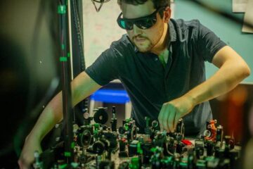
Engineers from Stanford and the University of Southern California have found a way to design circuits containing carbon nanotubes that should work even when many of the nanotubes are twisted or misaligned. Photo: Subhasish Mitra, Stanford University School of Engineering
Striking features
The Stanford design approach has two striking features in that it sacrifices virtually none of CNTs’ energy efficiency and it is also compatible with existing fabrication methods and infrastructure, pushing the technology a significant step toward commercialization.
“This transformative research is made all the more promising by the fact that it can co-exist with today’s mainstream silicon technologies, and leverage today’s manufacturing and system design infrastructure, providing the critical feature of economic viability,” said Betsy Weitzman of the Focus Center Research Program at the Semiconductor Research Corporation
The engineers next demonstrated the possibilities of their techniques by creating the essential components of digital integrated systems: arithmetic circuits and sequential storage, as well as the first monolithic three-dimensional integrated circuits with extreme levels of integration.
Stanford researchers, including undergraduates, in their “bunny suits” at the NSF-funded Stanford Nanofabrication facility. Photo: Subhasish Mitra, Stanford School of Engineering
The Stanford team’s work was featured recently as an invited paper at the prestigious International Electron Devices Meeting (IEDM) as well as a “keynote paper” in the prestigious IEEE Transactions on Computer-Aided Design of Integrated Circuits and Systems.
“Many researchers assumed that the way to live with imperfections in CNT manufacturing was through expensive fault-tolerance techniques. Through clever insights, Mitra and Wong have shown otherwise. Their inexpensive and practical methods can significantly improve CNT circuit robustness, and go a long way toward making CNT circuits viable,” said Sachin S. Sapatnekar, Editor-in-Chief, IEEE Transactions on CAD. “I anticipate high reader interest in the paper,” Sapatnekar noted.
Andrew Myers is associate director for communications for the Stanford University School of Engineering.
Editor's Note: This article first appeared as a “Behind the Scenes” feature on LiveScience in partnership with the National Science Foundation. The researchers depicted in Behind the Scenes have been supported by the National Science Foundation, the federal agency charged with funding basic research and education across all fields of science and engineering. Any opinions, findings, and conclusions or recommendations expressed in this material are those of the author and do not necessarily reflect the views of the National Science Foundation.
Media Contact
All latest news from the category: Physics and Astronomy
This area deals with the fundamental laws and building blocks of nature and how they interact, the properties and the behavior of matter, and research into space and time and their structures.
innovations-report provides in-depth reports and articles on subjects such as astrophysics, laser technologies, nuclear, quantum, particle and solid-state physics, nanotechnologies, planetary research and findings (Mars, Venus) and developments related to the Hubble Telescope.


Newest articles
Combatting disruptive ‘noise’ in quantum communication
In a significant milestone for quantum communication technology, an experiment has demonstrated how networks can be leveraged to combat disruptive ‘noise’ in quantum communications. The international effort led by researchers…

Stretchable quantum dot display
Intrinsically stretchable quantum dot-based light-emitting diodes achieved record-breaking performance. A team of South Korean scientists led by Professor KIM Dae-Hyeong of the Center for Nanoparticle Research within the Institute for…

Internet can achieve quantum speed with light saved as sound
Researchers at the University of Copenhagen’s Niels Bohr Institute have developed a new way to create quantum memory: A small drum can store data sent with light in its sonic…

